MC145170-1 Просмотр технического описания (PDF) - Motorola => Freescale
Номер в каталоге
Компоненты Описание
производитель
MC145170-1 Datasheet PDF : 27 Pages
| |||
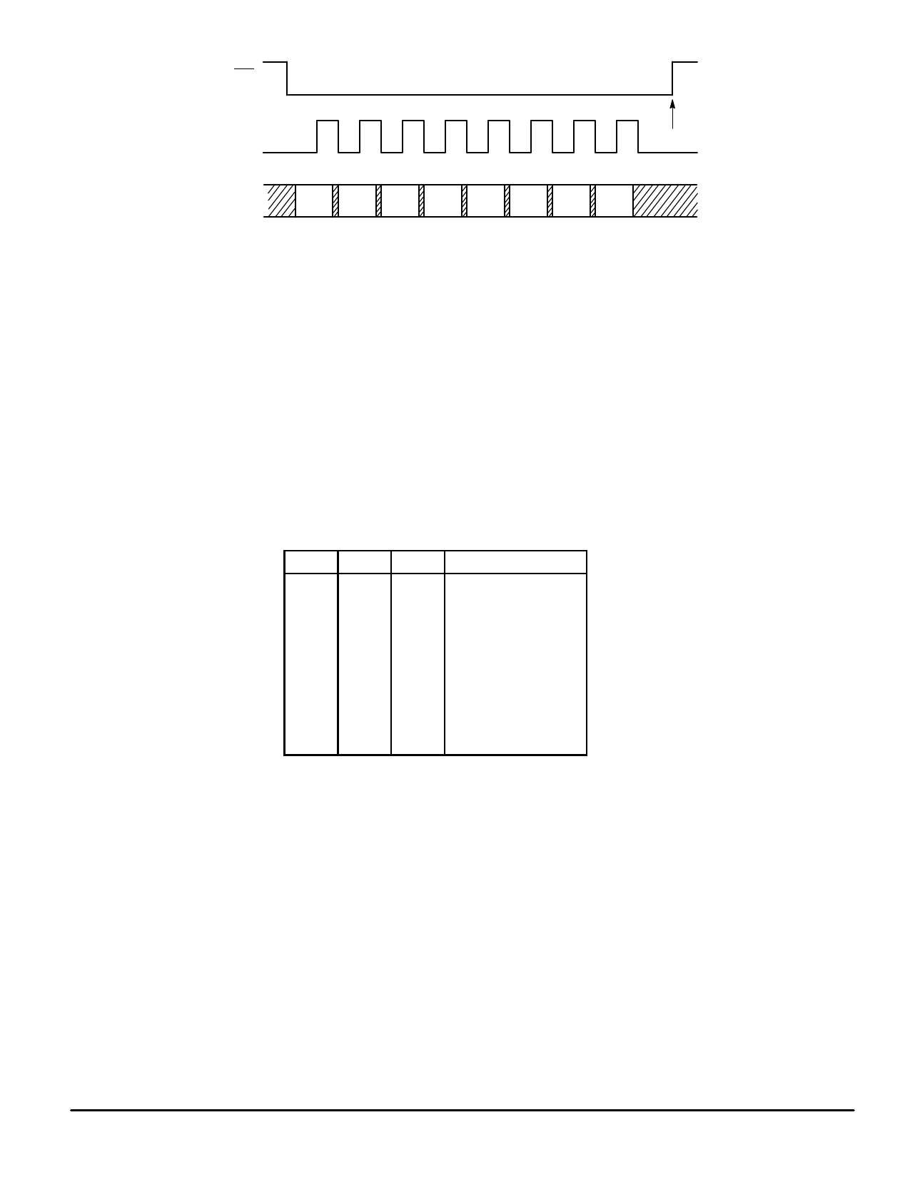
ENB
CLK
1
2
3
4
5
6
7
8
*
MSB
LSB
Din
C7 C6
C5
C4 C3
C2 C1
C0
* At this point, the new byte is transferred to the C register and stored. No other registers
are affected.
C7 — POL:
Selects the output polarity of the phase/frequency detectors. When set high, this bit inverts
PDout and interchanges the φR function with φV as depicted in Figure 17. Also see the phase
detector output pin descriptions for more information. This bit is cleared low at power up.
C6 — PDA/B:
Selects which phase/frequency detector is to be used. When set high, enables the output of
phase/frequency detector A (PDout) and disables phase/frequency detector B by forcing φR
and φV to the static high state. When cleared low, phase/frequency detector B is enabled (φR
and φV) and phase/frequency detector A is disabled with PDout forced to the high–impedance
state. This bit is cleared low at power up.
C5 — LDE: Enables the lock detector output when set high. When the bit is cleared low, the LD output is
forced to a static low level. This bit is cleared low at power up.
C4 – C2, OSC2 – OSC0: Reference output controls which determine the REFout characteristics as shown below. Upon
power up, the bits are initialized such that OSCin /8 is selected.
C4
C3
C2
REFout Frequency
0
0
0
dc (Static Low)
0
0
1
OSCin
0
1
0
OSCin /2
0
1
1
OSCin /4
1
0
0
OSCin /8
1
0
1
OSCin /16
1
1
0
OSCin /8
1
1
1
OSCin /16
C1 — fVE: Enables the fV output when set high. When cleared low, the fV output is forced to a static low
level. The bit is cleared low upon power up.
C0 — fRE: Enables the fR output when set high. When cleared low, the fR output is forced to a static low
level. The bit is cleared low upon power up.
Figure 14. C Register Access and Format (8 Clock Cycles are Used)
MOTOROLA
MC145170–1
11
Share Link: 