MCP3906AT-ISS Просмотр технического описания (PDF) - Microchip Technology
Номер в каталоге
Компоненты Описание
производитель
MCP3906AT-ISS Datasheet PDF : 26 Pages
| |||
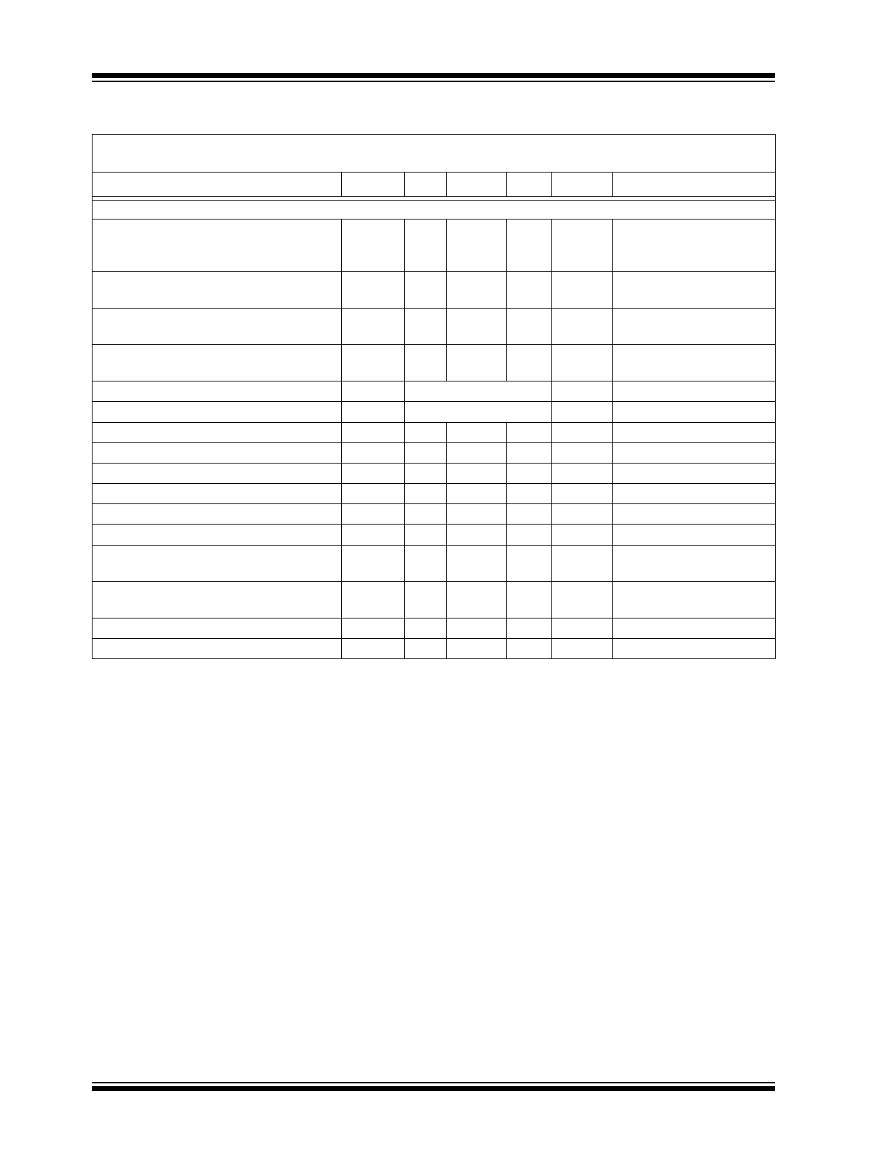
MCP3905A/05L/06A
TIMING CHARACTERISTICS
Electrical Specifications: Unless otherwise indicated, all parameters apply at AVDD = DVDD = 4.5V – 5.5V,
AGND, DGND = 0V, MCLK = 3.58 MHz; TA = -40°C to +85°C.
Parameter
Sym Min Typ Max Units
Comment
Frequency Output
FOUT0 and FOUT1 Pulse Width
tFW
(Logic Low) for MCP3905A, MCP3906A
devices
—
275
—
ms 984376 MCLK periods
(Note 1)
HFOUT Pulse Width for MCP3905A,
MCP3906A devices
tHW
—
90
—
ms 322160 MCLK periods
(Note 2)
FOUT0 and FOUT1 Pulse Width
(Logic Low) for MCP3905L device
tFW
—
130
—
ms 465344 MCLK periods
(Note 1)
HFOUT Pulse Width for MCP3905L
device
tHW
—
65
—
ms 232672 MCLK periods
(Note 2)
FOUT0 and FOUT1 Pulse Period
HFOUT Pulse Period
FOUT0 to FOUT1 Falling-Edge Time
FOUT0 to FOUT1 Min Separation
FOUT0 and FOUT1 Output High Voltage
FOUT0 and FOUT1 Output Low Voltage
HFOUT Output High Voltage
HFOUT Output Low Voltage
High-Level Input Voltage
(All Digital Input Pins)
tFP
tHP
tFS2
tFS
VOH
VOL
VOH
VOL
VIH
Refer to Equation 4-1
Refer to Equation 4-2
— 0.5 tFP —
— 4/MCLK —
4.5
—
—
—
—
0.5
4.0
—
—
—
—
0.5
2.4
—
—
s
s
V IOH = 10 mA, DVDD = 5.0V
V IOL = 10 mA, DVDD = 5.0V
V IOH = 5 mA, DVDD = 5.0V
V IOL = 5 mA, DVDD = 5.0V
V DVDD = 5.0V
Low Level Input Voltage
(All Digital Input Pins)
VIL
—
—
0.85
V DVDD = 5.0V
Input Leakage Current
Pin Capacitance
—
—
±3
µA VIN = 0, VIN = DVDD
—
—
10
pF Note 3
Note 1:
2:
If output pulse period (tFP) falls below 984376*2 MCLK periods for MCP3905A/6A and 465344*2 MCLK
periods for MCP3905L, then tFW = 1/2 tFP.
If output pulse period (tHP) falls below 322160*2 MCLK periods for MCP3905A/6A and 232672*2 MCLK
periods for MCP3905L, then tHW = 1/2 tHP. When F2, F1,F0 = 011, tHW is fixed to 18 µs (64 MCLK
periods).
3: Specified by characterization, not production tested.
DS22011A-page 4
© 2006 Microchip Technology Inc.
Share Link: 