ML674001 Просмотр технического описания (PDF) - Oki Electric Industry
Номер в каталоге
Компоненты Описание
производитель
ML674001 Datasheet PDF : 24 Pages
| |||
OKI Semiconductor
FEDL674001-01
ML674001/67Q4002/67Q4003
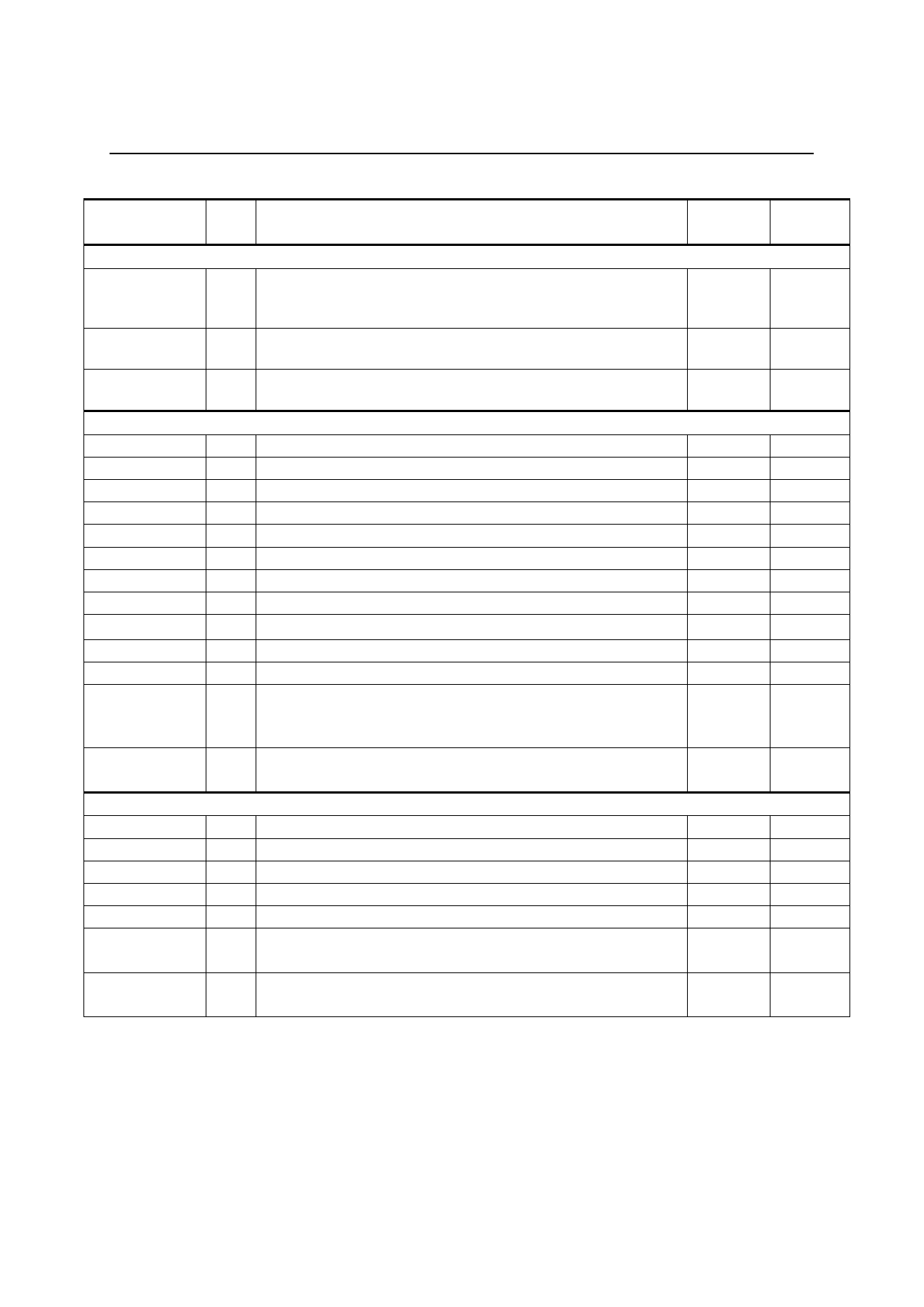
Pin Name
I/O
Description
External Bus
XA[23:19]
XA[18:0]
XD[15:0]
O Address bus to external RAM, external ROM, external I/O banks, and
external DRAM. After a reset, these pins are configured for their primary
function (PIOC[6:2]).
O Address bus to external RAM, external ROM, external I/O banks, and
external DRAM.
I/O Data bus to external RAM, external ROM, external I/O banks, and external
DRAM.
External bus control signals (ROM/SRAM/IO)
XROMCS_N
XRAMCS_N
XIOCS_N[0]
O ROM bank chip select
O SRAM bank chip select
O IO chip select 0
XIOCS_N[1]
XIOCS_N[2]
XIOCS_N[3]
O IO chip select 1
O IO chip select 2
O IO chip select 3
XOE_N
XWE_N
XBS_N[1:0]
O Output enable/ Read enable
O Write enable
O Byte select: XBS_N[1] is for MSB, XBS_N[0] is for LSB
XBWE_N[0]
XBWE_N[1]
O LSB Write enable
O MSB Write enable
XWR
XWAIT
O Data transfer direction for external bus, used when connecting to Motorola
I/O devices. This represent the secondary function of pin PIOC[7].
L: read , H: write. Available for I/O bank 0/1.
I External I/O bank 0/1, 2/3 WAIT signal.
This input permits access to devices slower than register settings.
External bus control signals (DRAM)
XRAS_N
O Row address strobe. Used for both EDO DRAM and SDRAM
XCAS_N
XSDCLK
XSDCKE
O Column address strobe signal (SDRAM)
O SDRAM clock (same frequency as internal HCLK)
O Clock enable (SDRAM)
XSDCS_N
XDQM[1]/XCAS_N[1]
XDQM[0]/XCAS_N[0]
O Chip select (SDRAM)
O Connected to SDRAM: DQM (MSB)
Connected to EDO DRAM: column address strobe signal (MSB)
O Connected to SDRAM: DQM (LSB)
Connected to EDO DRAM: column address strobe signal (LSB)
Primary /
Secondary
Secondary
—
—
—
—
—
—
—
—
—
—
—
—
—
Secondary
Secondary
Secondary
Secondary
Secondary
Secondary
Secondary
Secondary
Secondary
Logic
Positive
Positive
Positive
Negative
Negative
Negative
Negative
Negative
Negative
Negative
Negative
Negative
Negative
Negative
—
Positive
Negative
Negative
—
—
Negative
Positive/
Negative
Positive/
Negative
11/24
Share Link: 