TDA8763A Просмотр технического описания (PDF) - Philips Electronics
Номер в каталоге
Компоненты Описание
производитель
TDA8763A Datasheet PDF : 24 Pages
| |||
Philips Semiconductors
10-bit high-speed low-power ADC
Product specification
TDA8763A
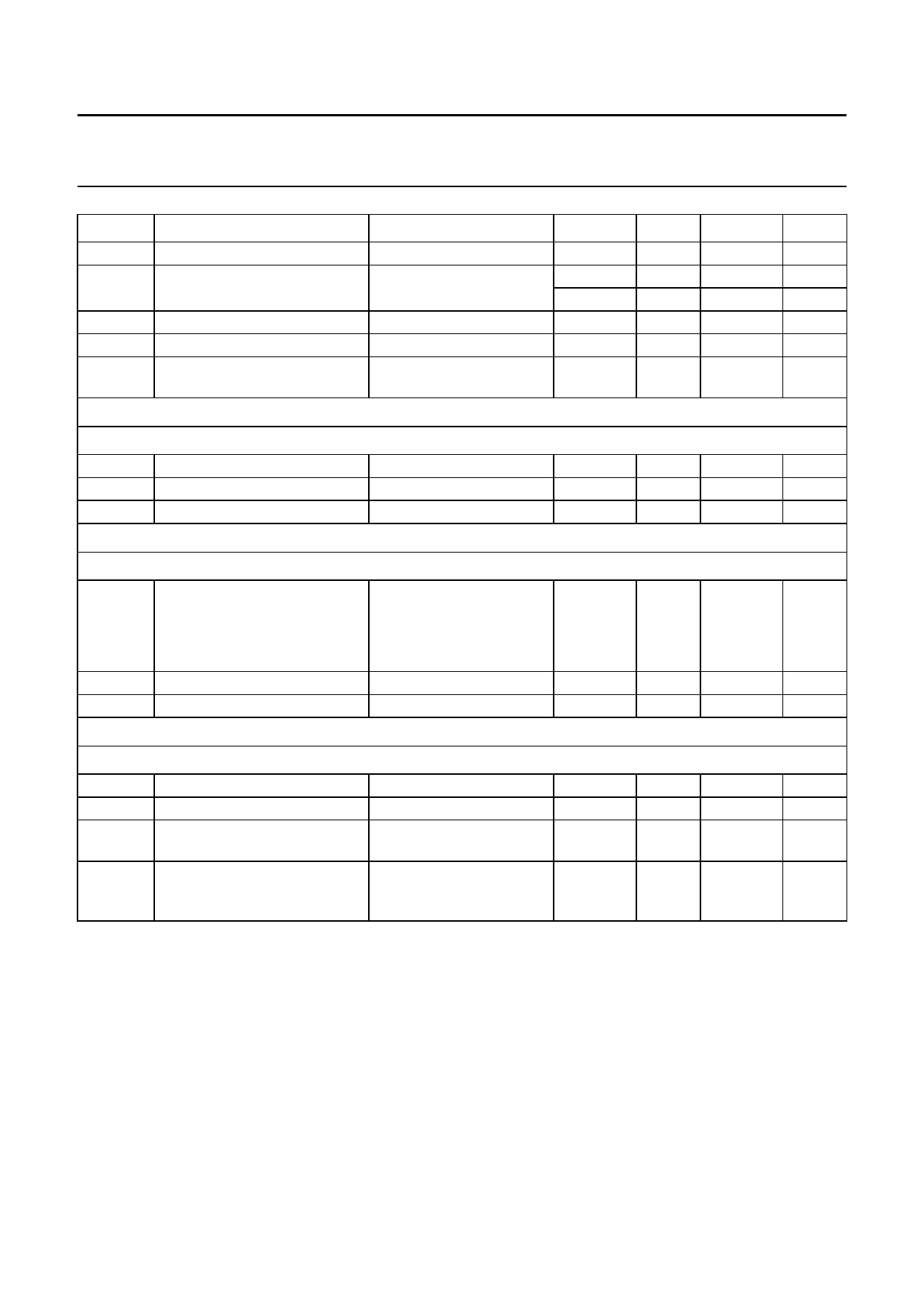
SYMBOL
PARAMETER
Rlad
TCRlad
resistor ladder
temperature coefficient of the
resistor ladder
Voffset(B)
Voffset(T)
Vi(p-p)
offset voltage BOTTOM
offset voltage TOP
analog input voltage
(peak-to-peak value)
CONDITIONS
MIN.
−
−
−
VRT − VRB = 2.37 V; note 2 −
VRT − VRB = 2.37 V; note 2 −
note 3
1.70
TYP.
245
1 860
456
175
175
2.02
Outputs
DIGITAL OUTPUTS D9 TO D0 AND IR (REFERENCED TO OGND)
VOL
LOW-level output voltage
IOL = 1 mA
VOH
HIGH-level output voltage
IOH = −1 mA
IOZ
output current in 3-state mode 0.5 V < Vo < VCCO
Switching characteristics
0
−
VCCO − 0.5 −
−20
−
CLOCK INPUT CLK; see Fig.4; note 1
fclk(max)
maximum clock frequency
TDA8763AM/3
30
−
TDA8763AM/4
TDA8763AM/5
40
−
50
−
tCPH
clock pulse width HIGH
full effective bandwidth 8.5
−
tCPL
clock pulse width LOW
full effective bandwidth 5.5
−
Analog signal processing
LINEARITY
INL
integral non-linearity
DNL
differential non-linearity
Eoffset
offset error
EG
gain error (from device to
device) using external
reference voltage
fclk = 40 MHz; ramp input −
fclk = 40 MHz; ramp input −
middle code; VRB = 1.3 V; −
VRT = 3.67 V
VRB = 1.3 V; VRT = 3.67 V; −
note 4
±0.8
±0.5
±1
±0.1
MAX.
−
−
−
−
−
2.55
0.5
VCCO
+20
−
−
−
−
−
±2.0
±0.9
−
−
UNIT
Ω
ppm
mΩ/K
mV
mV
V
V
V
µA
MHz
MHz
MHz
ns
ns
LSB
LSB
LSB
%
1999 Jan 06
8
Share Link: 