SC2595STRT(2007) Просмотр технического описания (PDF) - Semtech Corporation
Номер в каталоге
Компоненты Описание
производитель
SC2595STRT Datasheet PDF : 11 Pages
| |||
SC2595
POWER MANAGEMENT
Notes:
(1) Can be used for vias.
(2) Power up of AV , PV and V supplies.
CC
CC
DDQ
(a) The preferred mode of operation is when the AVCC, PVCC and VDDQ pins are tied together to a single supply.
(b) If and when AVCC, PVCC pins are tied to a supply separate to that of the VDDQ supply pin; then the VDDQ supply should
lead AVCC, PVCC supply or the VDDQ supply and the AVCC, PVCC supply should rise simultaneously.
(c) If the AVCC, PVCC and VDDQ supply pins are connected in a way such that, AVCC, PVCC supplies precedes VDDQ supply;
then V output precedes V . This can cause the SDRAM device to latch-up, which may cause permanent
TT
DDQ
damage to the SDRAM.
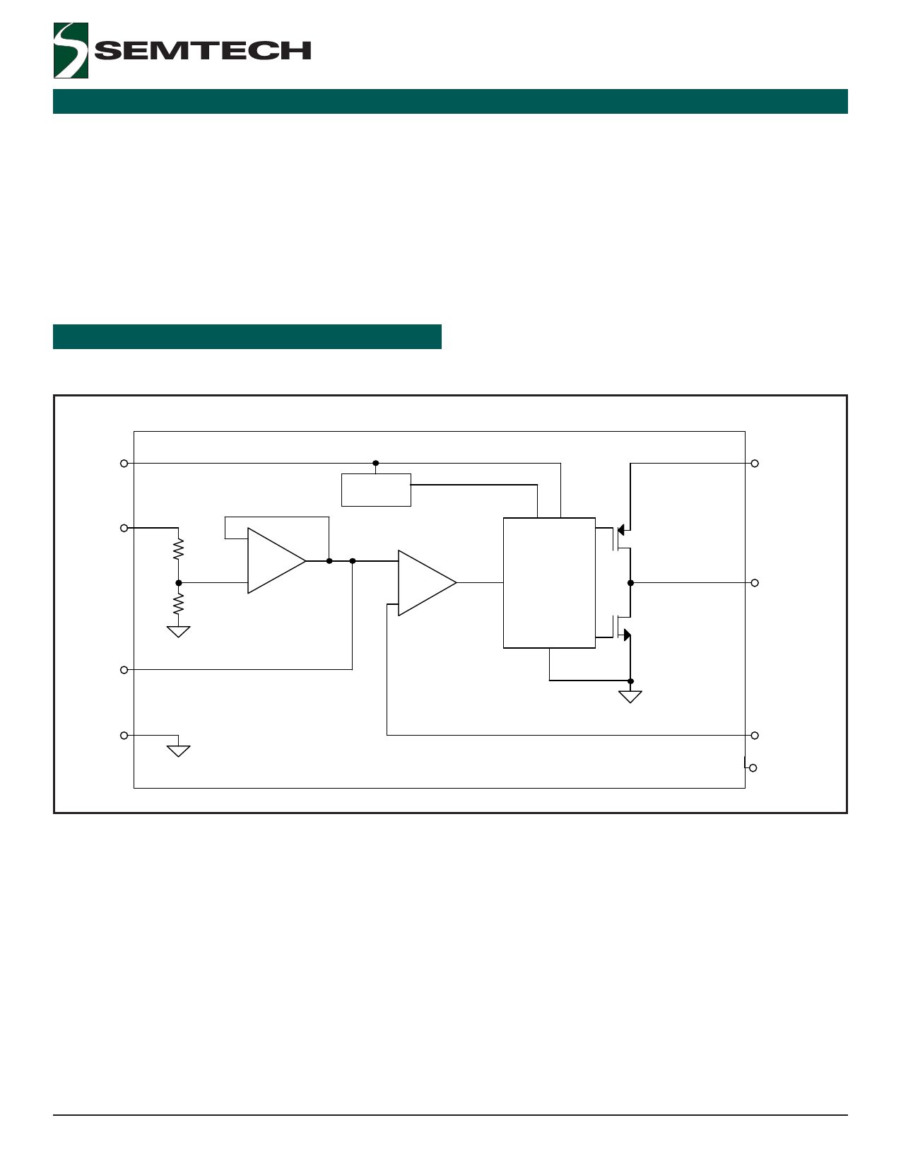
Block Diagram
AVCC
VDDQ
VREF
GND
-
OUT
+
UVLO
+
OUT
-
Driver
Circuit
PVCC
VTT
VSENSE
NC
© 2007 Semtech Corp.
5
www.semtech.com
Share Link: 