TSM006 Просмотр технического описания (PDF) - STMicroelectronics
Номер в каталоге
Компоненты Описание
производитель
TSM006 Datasheet PDF : 13 Pages
| |||
TSM006
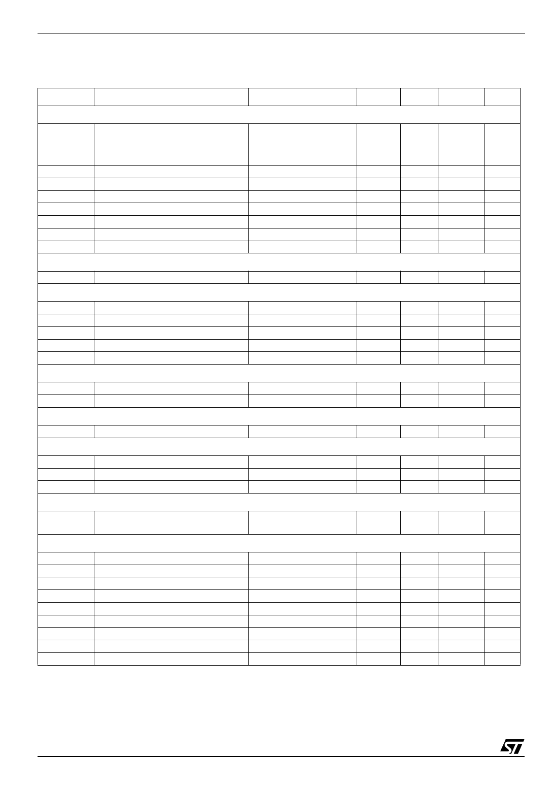
Electrical Characteristics
3 Electrical Characteristics
Tamb = 25°C, Vin=15V, Rt=39k, Ct=470pF, Rex=27k, Cfm=1nF unless otherwise specified
Symbol
Parameter
Test Condition
Min
Typ
Max
Unit
Main oscillator
8≤Vin≤20V, 0≤Ta≤105°C
Fosco Lower oscillating frequency
Vfm=GND
63
68
73
kHz
FoscL
Fjit
Ffm
Vthct
Vtlct
∆Vct
Idct1
Idct2
Upper oscillating frequency
Frequency jitter
Frequency modulation
Upper trip point
Lower trip point
Amplitude
Discharge current
Current at Ct in UVLO
Vfm=Vref
Fjit=Fosco - FoscL
Vfm=GND
Vfm=GND
Vfm=GND
Vct=2V
Vct=1V
57.6
62
66.4
kHz
6
7
8
kHz
4.5
kHz
3.0
V
1.4
V
1.6
V
300
µA
1
3
mA
Disable
Vdis Voltage threshold
2.5
2.65
2.8
V
Vref reference pin
Vref
∆Vline
∆Vload
∆Vtotal
Ios
Voltage reference
Line regulation
Load regulation
Total variation
Short circuit current
12V ≤ Vin ≤ 20V
1mA ≤ Iref ≤ 5mA
Line, load, temp
Vref=0
4.91
5.00
5.09
V
5
10
mV
10
20
mV
4.85
5.00
5.15
V
10
mA
Slope Compensation
IsinkCP Sink current
IsrcCP Source current
Vct=2.2V, VCslope=1V
90
µA
Vct=2.2V, VCslope=0V
2
mA
Comp
Icomp Source current
Vcomp=5V
0.5
0.6
0.7
mA
Current sense
Avcs
Vz1
PSRR
Gain
Maximum sensing voltage
Power supply voltage rejection ratio
0V ≤ Vcs ≤ 0.8V
Vcomp=5V
8V ≤ Vin ≤ 20V
2.85
3.00
3.15
0.9
1.0
1.1
V
70
dB
Leading edge blanking
LEB
Delay to output
Vcs = 0 to 2 V
Vcomp = 2 V
280
ns
Output
VOL1
VOL2
VOH1
VOH2
tr
tf
VOL3
Fout
DCmax
Output low voltage 1
Output low voltage 2
Output high voltage 1
Output high voltage 2
Rise time
Fall time
UVLO saturation
Output frequency
Maximum Duty Cycle
Iosink=20mA
1.0
V
Iosink=200mA
0.8
2.2
V
Iosource=20mA
Vin-2.0
V
Iosource=200mA
Vin-3.0
V
CL=1nF, 10% to 90%
70
100
ns
CL=1nF, 90% to 10%
40
60
ns
Vin=5V, Iosink=1mA
0.5
V
Option 1
Fosc
kHz
Option 1
77.5
%
4/13
Share Link: 