MCF53017CMJ240 Просмотр технического описания (PDF) - Freescale Semiconductor
Номер в каталоге
Компоненты Описание
производитель
MCF53017CMJ240 Datasheet PDF : 62 Pages
| |||
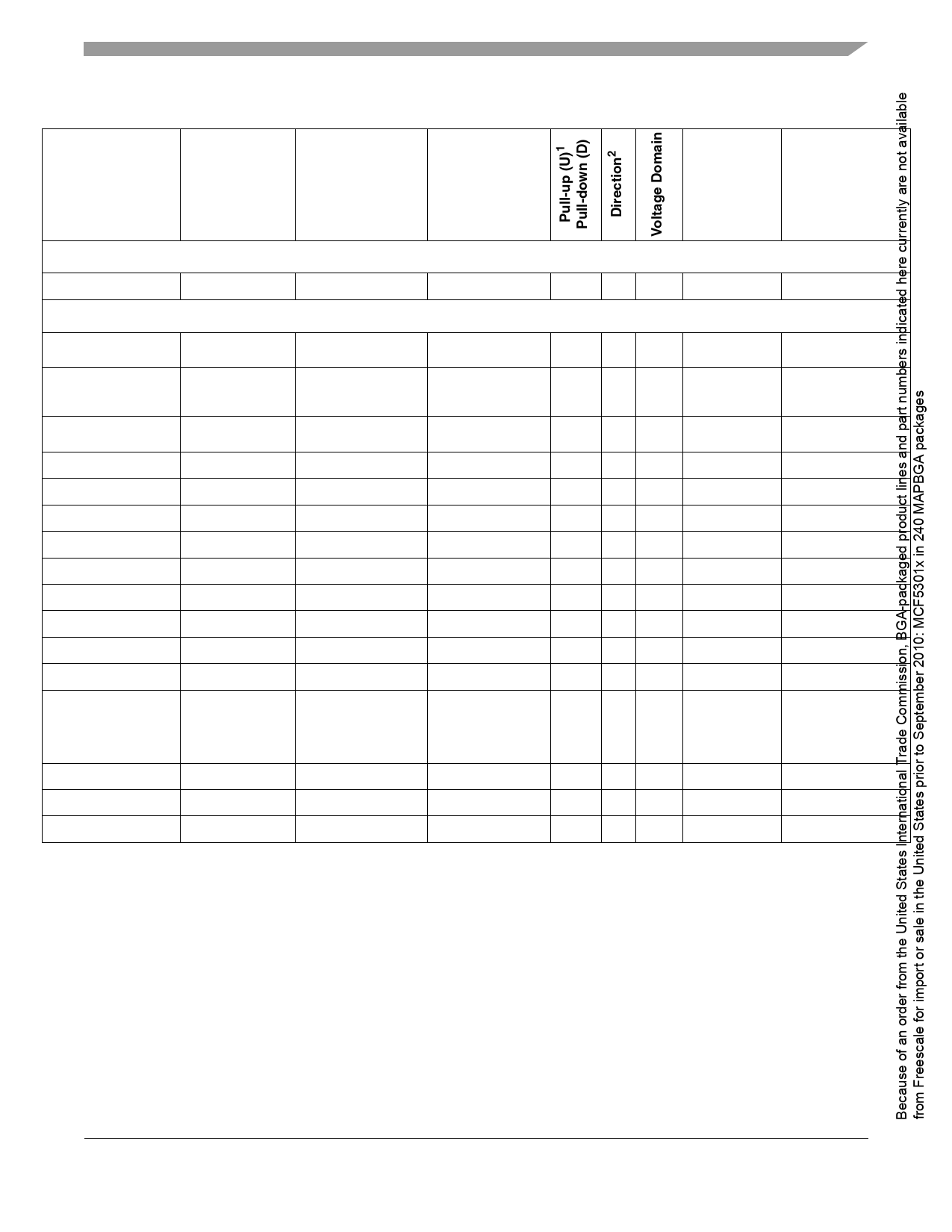
Pin Assignments and Reset States
Signal Name
Table 6. MCF5301x Signal Information and Muxing (continued)
GPIO
Alternate 1
Alternate 2
MCF53010
MCF53011
MCF53012
MCF53013
MCF53014
MCF53015
MCF53016
MCF53017
Test
208 LQFP
256 MAPBGA
TEST
—
—
—
D
I EVDD
146
F12
Power Supplies
IVDD
—
—
—
—
—
— 16, 44, 69, 77, 128, E9, F8, F9, H5, H6, H11,
169, 193
H12, J6, J11, L8, L9
EVDD
—
—
—
—
—
— 9, 24, 26, 40, 47,
F5, G6, G11, G12,
51, 54, 57, 74, 126, J12, K6, K11, K12,
139, 195
L5-7, L10-12, M5-7, M12
SD_VDD
—
—
—
—
— — 7, 102, 116, 156, E5, E6, E10-12, F6, F7,
163, 181, 208
F10, F11
VDD_OSC_A_PLL
—
—
—
— ——
46
M4
VDD_USBO
—
—
—
— ——
147
E7
VDD_USBH
—
—
—
— ——
—
E8
VDD_RTC
—
—
—
— ——
—
AVDD_CODEC
—
—
—
— ——
80
N8
AVDD_SPKR
—
—
—
— ——
—
T8
VDD_EPM
—
—
—
— ——
96
M9
VSTBY_SRAM
—
—
—
— ——
—
L2
VSTBY_RTC
—
—
—
— ——
—
L4
VSS
—
—
—
—
— — 8, 15, 25, 39, 45, A1, A16, G7-10, H7-10,
48, 52, 53, 56, 68, J7-10, K7-10, T1, T16
73, 76, 101, 117,
138, 168, 180, 192,
194
VSS_CODEC
—
—
—
— ——
83
N10
AVSS_SPKR_HDST
—
—
—
— ——
—
T6
AVSS_SPKR_HP
—
—
—
— ——
—
T10
1 Pull-ups are generally only enabled on pins with their primary function, except as noted.
2 Refers to pin’s primary function.
3 Enabled only in oscillator bypass mode (internal crystal oscillator is disabled).
4 The edge port 1 signals are the primary functions on two sets of pins (IRQ1FECn and IRQ1DEBUGn). If an IRQ1 function is configured on
both pins, the IRQ1FECn pin takes priority. The corresponding IRQ1DEBUGn pin is disconnected internally from the edge port 1 module.
5 GPIO functionality is determined by the edge port module. The GPIO module is only responsible for assigning the alternate functions.
6 If JTAG_EN is asserted, these pins default to alternate 1 (JTAG) functionality. The GPIO module is not responsible for assigning these pins.
MCF5301x Data Sheet, Rev. 5
Freescale Semiconductor
Preliminary—Subject to Change Without Notice
15
Share Link: 