IRL3803 –ü—Ä–æ—Å–º–æ—Ç—Ä —Ç–µ—Ö–Ω–∏—á–µ—Å–∫–æ–≥–æ –æ–ø–∏—Å–∞–Ω–∏—è (PDF) - Unspecified
–ù–æ–º–µ—Ä –≤ –∫–∞—Ç–∞–ª–æ–≥–µ
–ö–æ–º–ø–æ–Ω–µ–Ω—Ç—ã –û–ø–∏—Å–∞–Ω–∏–µ
–ø—Ä–æ–∏–∑–≤–æ–¥–∏—Ç–µ–ª—å
IRL3803 Datasheet PDF : 7 Pages
| |||
IRL3803
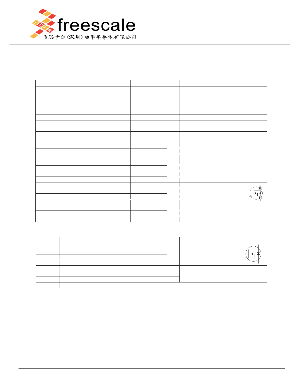
Electrical Characteristics @ TJ = 25°C (unless otherwise specified)
Parameter
Min. Typ. Max. Units
Conditions
V(BR)DSS Drain-to-Source Breakdown Voltage
30 ––– ––– V VGS = 0V, ID = 250µA
∆V(BR)DSS/∆TJ Breakdown Voltage Temp. Coefficient ––– 0.052 ––– V/°C Reference to 25°C, ID = 1mA
RDS(on)
Static Drain-to-Source On-Resistance
––– ––– 0.006 Ω VGS = 10V, ID = 71A „
––– ––– 0.009
VGS = 4.5V, ID = 59A „
VGS(th)
Gate Threshold Voltage
1.0 ––– ––– V VDS = VGS, ID = 250µA
gfs
Forward Transconductance
55 ––– ––– S VDS = 25V, ID = 71A
IDSS
Drain-to-Source Leakage Current
––– ––– 25 µA VDS = 30V, VGS = 0V
––– ––– 250
VDS = 24V, VGS = 0V, TJ = 150°C
IGSS
Gate-to-Source Forward Leakage
Gate-to-Source Reverse Leakage
––– ––– 100 nA VGS = 16V
––– ––– -100
VGS = -16V
Qg
Total Gate Charge
––– ––– 140
ID = 71A
Qgs
Gate-to-Source Charge
––– ––– 41 nC VDS = 24V
Qgd
Gate-to-Drain ("Miller") Charge
––– ––– 78
VGS = 4.5V, See Fig. 6 and 13 „
td(on)
Turn-On Delay Time
––– 14 –––
VDD = 15V
tr
td(off)
tf
Rise Time
Turn-Off Delay Time
Fall Time
––– 230 –––
––– 29 –––
ns
ID = 71A
RG = 1.3Ω, VGS = 4.5V
––– 35 –––
RD = 0.20Ω, See Fig. 10 „
LD
Internal Drain Inductance
LS
Internal Source Inductance
––– 4.5 –––
––– 7.5 –––
Between lead,
6mm (0.25in.)
nH from package
and center of die contact
D
G
S
Ciss
Input Capacitance
––– 5000 –––
VGS = 0V
Coss
Output Capacitance
––– 1800 ––– pF VDS = 25V
Crss
Reverse Transfer Capacitance
––– 880 –––
ƒ = 1.0MHz, See Fig. 5
Source-Drain Ratings and Characteristics
Parameter
IS
Continuous Source Current
(Body Diode)
ISM
Pulsed Source Current
(Body Diode) 
VSD
Diode Forward Voltage
trr
Reverse Recovery Time
Qrr
Reverse RecoveryCharge
ton
Forward Turn-On Time
Min. Typ. Max. Units
Conditions
MOSFET symbol
––– ––– 140… A showing the
––– ––– 470
integral reverse
p-n junction diode.
D
G
S
––– ––– 1.3 V TJ = 25°C, IS = 71A, VGS = 0V „
––– 120 180 ns TJ = 25°C, IF = 71A
––– 450 680 nC di/dt = 100A/µs „
Intrinsic turn-on time is negligible (turn-on is dominated by LS+LD)
Notes:
 Repetitive rating; pulse width limited by
max. junction temperature. ( See fig. 11 )
‚ VDD = 15V, starting TJ = 25°C, L = 180µH
RG = 25Ω, IAS = 71A. (See Figure 12)
ƒ ISD ≤ 71A, di/dt ≤ 130A/µs, VDD ≤ V(BR)DSS,
TJ ≤ 175°C
„ Pulse width ≤ 300µs; duty cycle ≤ 2%.
¬Ö Caculated continuous current based on maximum allowable
junction temperature;for recommended current-handling of the
package refer to Design Tip # 93-4
2/8
www.freescale.net.cn
Share Link: 