M37225M8 Просмотр технического описания (PDF) - Renesas Electronics
Номер в каталоге
Компоненты Описание
производитель
M37225M8
Renesas Electronics
M37225M8 Datasheet PDF : 126 Pages
| |||
M37225M6/M8/MA/MC-XXXSP, M37225ECSP
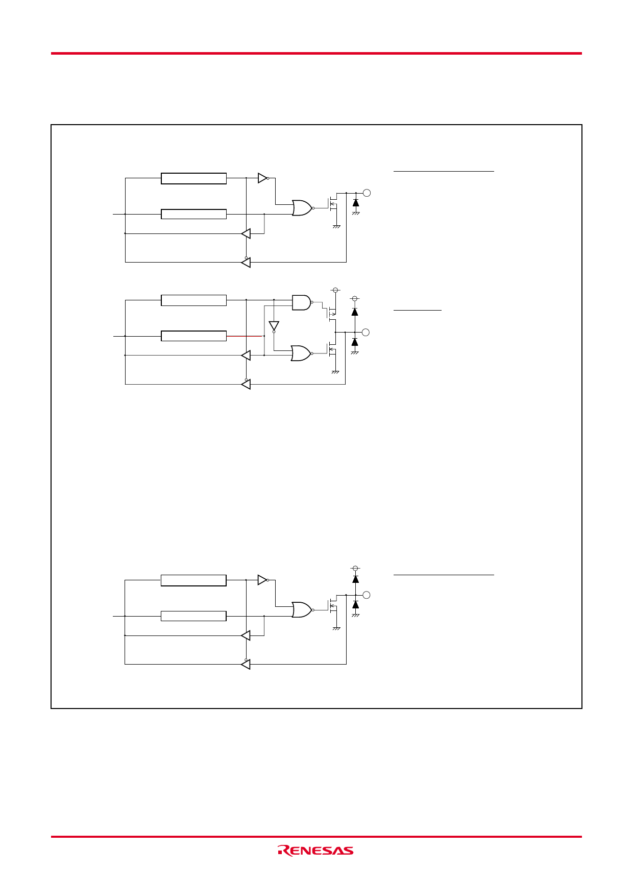
Ports P00–P05
Data bus
Direction register
Port latch
Ports P1, P2, P30, P31
Direction register
Data bus
Port latch
Ports P06, P07, P32
Data bus
Direction register
Port latch
Fig. 7.1 I/O Pin Block Diagram (1)
Rev.1.00 Nov 01, 2000 page 9 of 124
REJ03B0136-0100Z
N-channel open-drain output
Ports P00–P05
Note : Each port is also used as follows :
P00–P05 : PWM0–PWM5
CMOS output
Ports P1, P2, P30, P31, P35
Notes 1: Each port is also used as follows :
P10 : OUT2/AD8 P22 : SIN
P11 : SCL1
P23 : TIM3
P12 : SCL2
P24 : TIM2
P13 : SDA1
P30 : A-D5
P14 : SDA2
P31 : A-D6
P15 : INT3/A-D1 P35 : DA1
P16 : A-D2
P17 : DA2/A-D3
P20 : SCLK
P21 : SOUT/(SIN)
2: Either CMOS output or N-channel open-
drain output structure can be selected as
ports P30, P31 and P35 (when selecting
N-channel open-drain, it is the same with
N-channel open-drain output below).
N-channel open-drain output
Ports P06, P07, P32
Note : Each port is also used as follows :
P06 : INT2/A-D4
P07 : INT1
Share Link: 