MC14572UB Просмотр технического описания (PDF) - ON Semiconductor
Номер в каталоге
Компоненты Описание
производитель
MC14572UB Datasheet PDF : 5 Pages
| |||
MC14572UB
Hex Gate
The MC14572UB hex functional gate is constructed with MOS
P−channel and N−channel enhancement mode devices in a single
monolithic structure. These complementary MOS logic gates find
primary use where low power dissipation and/or high noise immunity
is desired. The chip contains four inverters, one NOR gate and one
NAND gate.
Features
• Diode Protection on All Inputs
• Single Supply Operation
• Supply Voltage Range = 3.0 Vdc to 18 Vdc
• NOR Input Pin Adjacent to VSS Pin to Simplify Use As An Inverter
• NAND Input Pin Adjacent to VDD Pin to Simplify Use As An
Inverter
• NOR Output Pin Adjacent to Inverter Input Pin For OR Application
• NAND Output Pin Adjacent to Inverter Input Pin For AND
Application
• Capable of Driving Two Low−Power TTL Loads or One
Low−Power Schottky TTL Load over the Rated Temperature
Range
• NLV Prefix for Automotive and Other Applications Requiring
Unique Site and Control Change Requirements; AEC−Q100
Qualified and PPAP Capable*
• This Device is Pb−Free and is RoHS Compliant
MAXIMUM RATINGS (Voltages Referenced to VSS)
Parameter
Symbol
Value
Unit
DC Supply Voltage Range
VDD −0.5 to +18.0 V
Input or Output Voltage Range
(DC or Transient)
Vin, Vout − 0.5 to VDD V
+ 0.5
Input or Output Current (DC or Transient) Iin, Iout
±10
mA
per Pin
Power Dissipation, per Package (Note 1)
PD
500
mW
Ambient Temperature Range
TA
−55 to +125 °C
Storage Temperature Range
Tstg
−65 to +150 °C
Lead Temperature (8−Second Soldering)
TL
260
°C
Stresses exceeding those listed in the Maximum Ratings table may damage the
device. If any of these limits are exceeded, device functionality should not be
assumed, damage may occur and reliability may be affected.
1. Temperature Derating: “D/DW” Package: –7.0 mW/_C From 65_C To 125_C
This device contains protection circuitry to guard against damage due to high
static voltages or electric fields. However, precautions must be taken to avoid
applications of any voltage higher than maximum rated voltages to this
high−impedance circuit. For proper operation, Vin and Vout should be constrained
to the range VSS ≤ (Vin or Vout) ≤ VDD.
Unused inputs must always be tied to an appropriate logic voltage level
(e.g., either VSS or VDD). Unused outputs must be left open.
http://onsemi.com
1
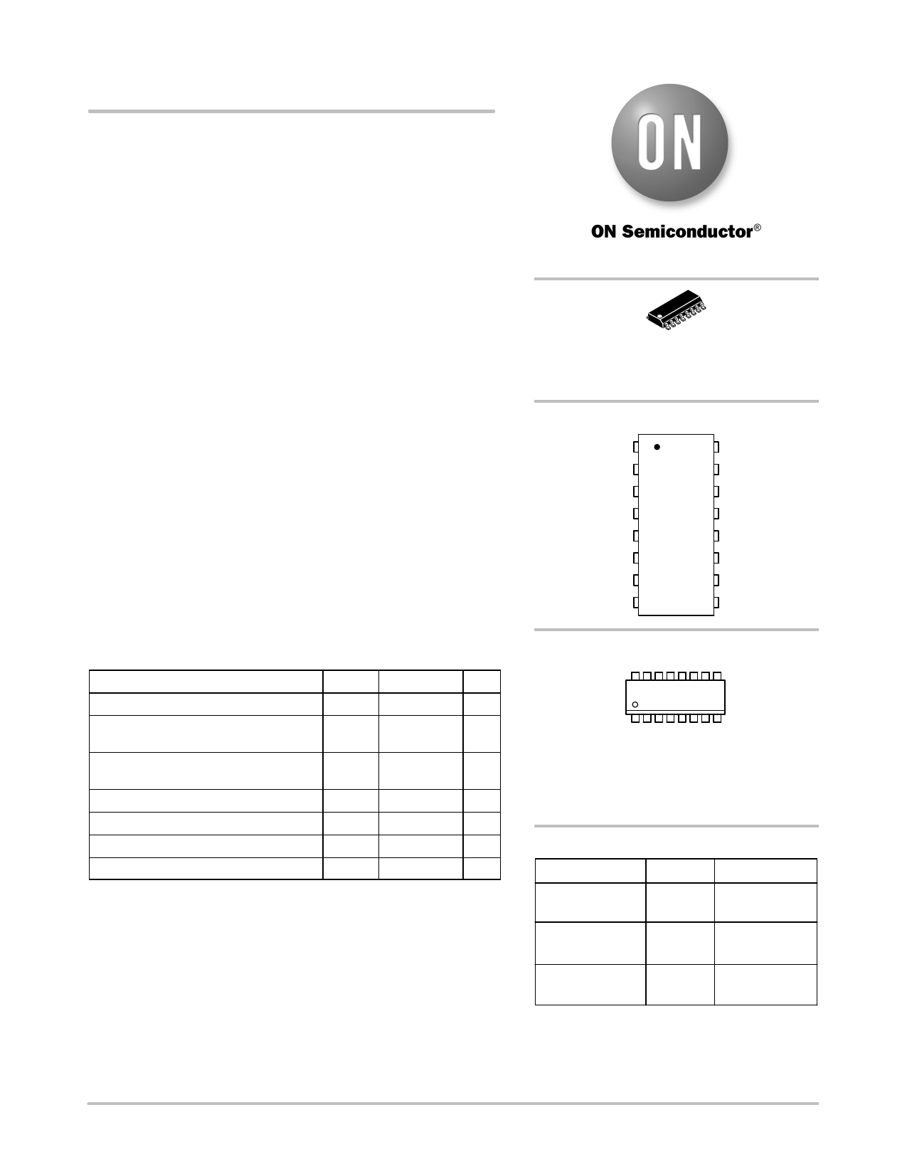
SOIC−16
D SUFFIX
CASE 751B
PIN ASSIGNMENT
OUTA 1
INA 2
OUTB 3
INB 4
OUTC 5
IN 1C 6
IN 2C 7
VSS 8
16 VDD
15 IN 2F
14 IN 1F
13 OUTF
12 INE
11 OUTE
10 IND
9 OUTD
MARKING DIAGRAM
16
14572UG
AWLYWW
1
A
= Assembly Location
WL = Wafer Lot
YY
= Year
WW = Work Week
G
= Pb−Free Package
ORDERING INFORMATION
Device
Package
Shipping†
MC14572UBDG
SOIC−16
(Pb−Free)
48 Units / Rail
MC14572UBDR2G SOIC−16 2500/Tape & Reel
(Pb−Free)
NLV14572UBDR2G* SOIC−16 2500/Tape & Reel
(Pb−Free)
†For information on tape and reel specifications,
including part orientation and tape sizes, please
refer to our Tape and Reel Packaging Specifications
Brochure, BRD8011/D.
© Semiconductor Components Industries, LLC, 2014
1
July, 2014 − Rev. 10
Publication Order Number:
MC14572UB/D
Share Link: 