LM308AD Просмотр технического описания (PDF) - ON Semiconductor
Номер в каталоге
Компоненты Описание
производитель
LM308AD Datasheet PDF : 8 Pages
| |||
LM308A
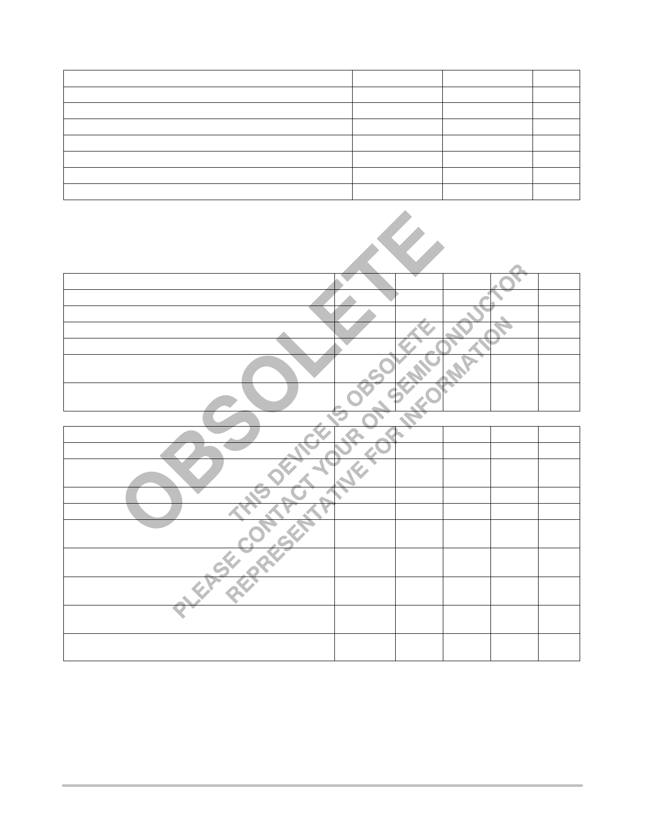
MAXIMUM RATINGS (TA = +25°C, unless otherwise noted.)
Rating
Symbol
Value
Unit
Power Supply Voltage
Input Voltage (Note 1)
Input Differential Current (Note 2)
VCC, VEE
VI
IID
±18
Vdc
±15
V
±10
mA
Output Short Circuit Duration
tSC
Indefinite
−
Operating Ambient Temperature Range
TA
0 to +70
°C
Storage Temperature Range
Tstg
−65 to +150
°C
Junction Temperature
TJ
+150
°C
1. For supply voltages less than ±15 V, the maximum input voltage is equal to the supply voltage.
2. The inputs are shunted with back−to−back diodes for overvoltage protection. Therefore, excessive current will flow if a differential input
voltage in excess of 1.0 V is applied between the inputs, unless some limiting resistance is used.
ELECTRICAL CHARACTERISTICS (Unless otherwise noted these specifications apply for supply voltages of +5.0 V ≤ VCC ≤
+15 V and −5.0 V ≥ VEE ≥ −15 V, TA = +25°C.)
Characteristic
Symbol
Min
Typ
Max
Unit
Input Offset Voltage
VIO
−
0.3
0.5
mV
Input Offset Current
IIO
−
0.2
1.0
nA
Input Bias Current
IIB
−
1.5
7.0
nA
Input Resistance
ri
10
40
−
MΩ
Power Supply Currents
(VCC = +15 V, VEE = −15 V)
ICC, IEE
−
±0.3
±0.8
mA
Large Signal Voltage Gain
(VCC = +15 V, VEE = −15 V, VO = ±10 V, RL ≥ 10 kΩ)
AVOL
80
300
−
V/mV
The following specifications apply over the operating temperature range.
Input Offset Voltage
VIO
−
−
0.73
mV
Input Offset Current
IIO
−
−
1.5
nA
Average Temperature Coefficient of Input Offset Voltage
TA (min) ≤ TA ≤ TA (max)
Average Temperature Coefficient of Input Offset Current
∆VIO/∆T
−
∆IIO/∆T
−
1.0
5.0
µV/°C
2.0
10
pA/°C
Input Bias Current
IIB
−
−
10
nA
Large Signal Voltage Gain
(VCC +15 V, VEE = −15 V, VO = ±10 V, RL ≥ 10 kΩ)
Input Voltage Range
(VCC = +15 V, VEE = −15 V)
AVOL
60
−
VICR
±14
−
−
V/mV
−
V
Common Mode Rejection
(RS ≤ 50 kΩ)
CMR
96
110
−
dB
Supply Voltage Rejection
(RS ≤ 50 kΩ)
Output Voltage Range
(VCC = +15 V, VEE = −15 V, RL = 10 kΩ)
PSR
96
110
−
dB
VOR
±13
±14
−
V
http://onsemi.com
2
Share Link: 