LD1117S28 Просмотр технического описания (PDF) - STMicroelectronics
Номер в каталоге
Компоненты Описание
производитель
LD1117S28 Datasheet PDF : 28 Pages
| |||
LD1117 SERIES
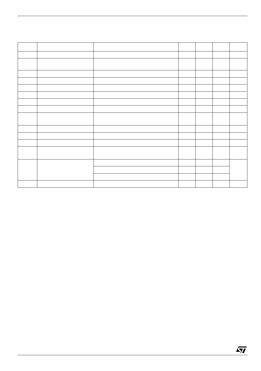
Table 12: Electrical Characteristics Of LD1117#12C (refer to the test circuits, TJ = 0 to 125°C,
CO = 10 µF, R = 120 Ω between GND and OUT pins, unless otherwise specified)
Symbol
Parameter
Vref Reference Voltage
Vref Reference Voltage
∆VO
∆VO
∆VO
∆VO
Vin
Iadj
∆Iadj
Line Regulation
Load Regulation
Temperature Stability
Long Term Stability
Operating Input Voltage
Adjustment Pin Current
Adjustment Pin Current
Change
IO(min)
IO
eN
SVR
Minimum Load Current
Output Current
Output Noise (%VO)
Supply Voltage Rejection
Vd Dropout Voltage
Thermal Regulation
Test Conditions
Vin - VO= 2V IO = 10 mA TJ = 25°C
IO = 10 to 800 mA
V
Vin - VO= 1.4 to 10
Vin - VO = 1.5 to 13.75 V
IO = 10 mA
Vin - VO = 3 V
IO = 10 to 800 mA
1000 hrs, TJ = 125°C
Vin ≤ 15 V
Vin - VO = 1.4 to 10 V
IO = 10 to 800 mA
Vin = 15 V
Vin - VO = 5 V
TJ = 25°C
B =10Hz to 10KHz TJ = 25°C
IO = 40 mA f = 120Hz
TJ = 25°C
Vin - VO = 3 V
Vripple = 1 VPP
IO = 100 mA
TJ = 0 to 125°C
IO = 500 mA
TJ = 0 to 125°C
IO = 800 mA
TJ = 0 to 125°C
Ta = 25°C 30ms Pulse
Min.
1.176
1.120
800
60
Typ.
1.20
1.20
0.5
0.3
60
1
2
950
0.003
75
1
1.05
1.10
0.01
Max.
1.224
1.280
1
1
15
120
5
5
1300
1.1
1.2
1.3
0.1
Unit
V
V
%
%
%
%
V
µA
µA
mA
mA
%
dB
V
%/W
8/28
Share Link: 