M27C4002-12XB1 Просмотр технического описания (PDF) - STMicroelectronics
Номер в каталоге
Компоненты Описание
производитель
M27C4002-12XB1 Datasheet PDF : 24 Pages
| |||
M27C4002
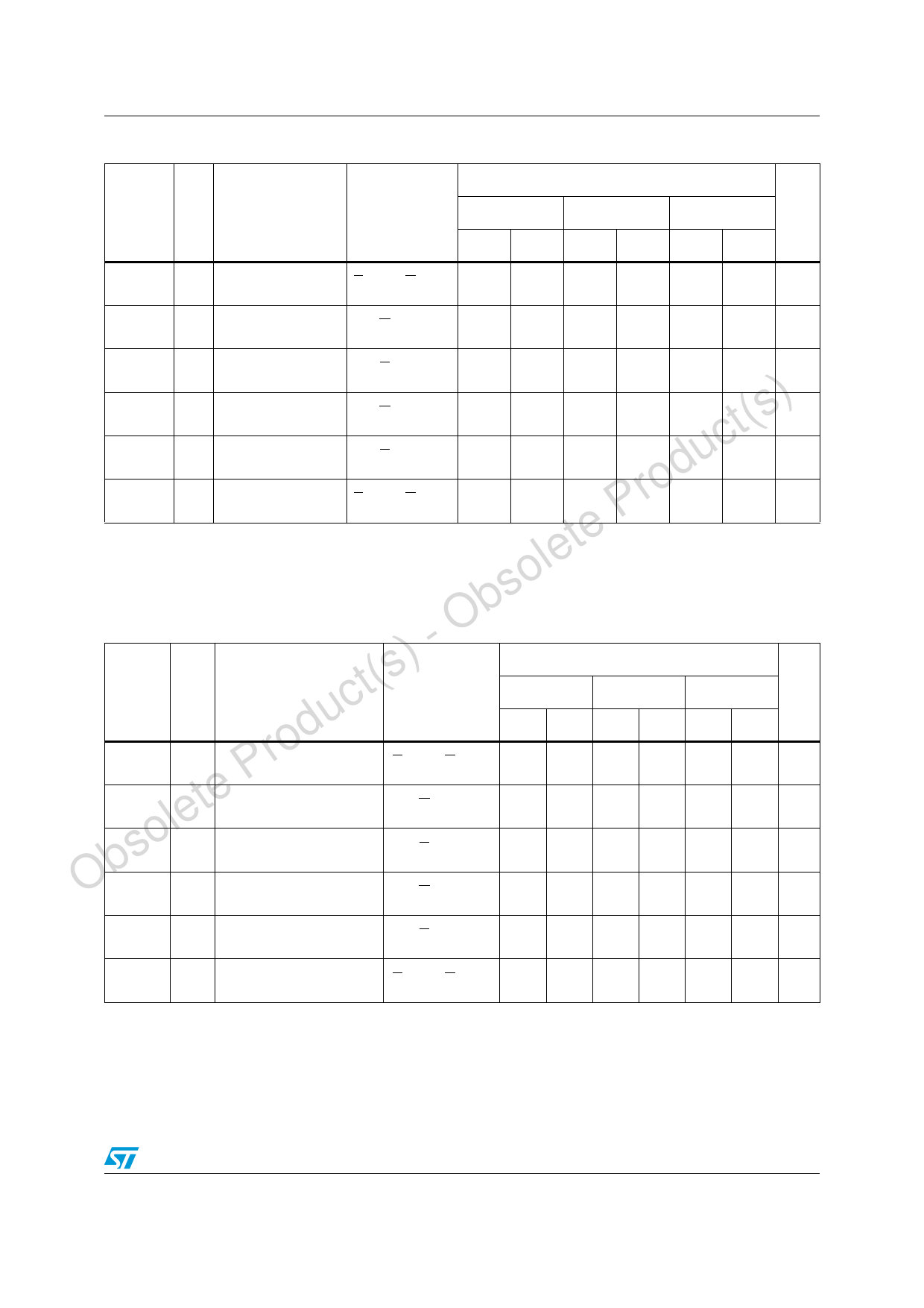
DC and AC parameters
Table 9. Read Mode AC Characteristics 1(1)(2)
Symbol Alt
Parameter
Test Condition
- 45(3)
M27C4002
-60 (3)
-70
Unit
Min Max Min Max Min Max
tAVQV
tACC
Address Valid to
Output Valid
E = VIL, G = VIL
45
60
70 ns
tELQV
tCE
Chip Enable Low to
Output Valid
G = VIL
45
60
70 ns
tGLQV
tOE
Output Enable Low
to Output Valid
E = VIL
25
30
t(s) tEHQZ(4)
tDF
Chip Enable High to
Output Hi-Z
G = VIL
0
30
0
30
0
uc tGHQZ(4)
tDF
Output Enable High
to Output Hi-Z
E = VIL
0
30
0
30
0
rod tAXQX
tOH
Address Transition
to Output Transition
E = VIL, G = VIL
0
0
0
te P 1. TA = 0 to 70°C or –40 to 85°C; VCC = 5V ± 5% or 5V ± 10%; VPP = VCC.
le 2. VCC must be applied simultaneously with or before VPP and removed simultaneously or after VPP.
o 3. Speed obtained with High Speed AC measurement conditions.
s 4. Sampled only, not 100% tested.
Ob Table 10. Read Mode AC Characteristics 2(1)(2)
) - M27C4002
35 ns
30 ns
30 ns
ns
t(s Symbol Alt
Parameter
Test Condition
-80
-90
-10
Unit
roduc tAVQV
tACC
Address Valid to Output
Valid
te P tELQV
tCE
Chip Enable Low to
Output Valid
sole tGLQV
tOE
Output Enable Low to
Output Valid
ObtEHQZ(3)
tDF
Chip Enable High to
Output Hi-Z
Min Max Min Max Min Max
E = VIL, G = VIL
80
90
100 ns
G = VIL
80
90
100 ns
E = VIL
40
40
50 ns
G = VIL
0 30 0 30 0 30 ns
tGHQZ(3)
tDF
Output Enable High to
Output Hi-Z
E = VIL
0 30 0 30 0 30 ns
tAXQX
tOH
Address Transition to
Output Transition
E = VIL, G = VIL 0
0
0
ns
1. TA = 0 to 70°C or –40 to 85°C; VCC = 5V ± 5% or 5V ± 10%; VPP = VCC.
2. VCC must be applied simultaneously with or before VPP and removed simultaneously or after VPP.
3. Sampled only, not 100% tested.
15/24
Share Link: 