IRF150 Просмотр технического описания (PDF) - Semelab - > TT Electronics plc
Номер в каталоге
Компоненты Описание
производитель
IRF150 Datasheet PDF : 2 Pages
| |||
IRF150
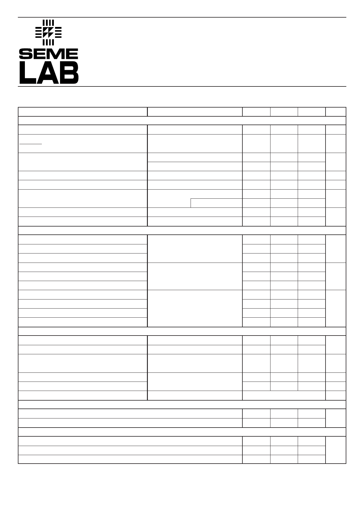
ELECTRICAL CHARACTERISTICS (Tcase = 25°C unless otherwise stated)
Parameter
Test Conditions
Min.
STATIC ELECTRICAL RATINGS
BVDSS Drain – Source Breakdown Voltage VGS = 0
ID = 1mA
100
∆BVDSS Temperature Coefficient of
Reference to 25°C
∆TJ Breakdown Voltage
ID = 1mA
Static Drain – Source On–State
RDS(on) Resistance 1
VGS = 10V
VGS = 10V
ID = 24A
ID = 38A
VGS(th) Gate Threshold Voltage
VDS = VGS
ID = 250mA
2
gfs
Forward Transconductance 1
VDS ≥ 15V
IDS = 24A
9
IDSS Zero Gate Voltage Drain Current
VGS = 0
VDS = 0.8BVDSS
TJ = 125°C
IGSS Forward Gate – Source Leakage
VGS = 20V
IGSS Reverse Gate – Source Leakage
VGS = –20V
DYNAMIC CHARACTERISTICS
Ciss Input Capacitance
VGS = 0
Coss Output Capacitance
VDS = 25V
Crss Reverse Transfer Capacitance
f = 1MHz
Qg
Total Gate Charge
VGS = 10V
50
Qgs Gate – Source Charge
ID = 38A
8
Qgd Gate – Drain (“Miller”) Charge
VDS = 0.5BVDSS
25
td(on)
tr
td(off)
tf
Turn–On Delay Time
Rise Time
Turn–Off Delay Time
Fall Time
VDD = 50V
ID = 38A
RG = 2.35Ω
SOURCE – DRAIN DIODE CHARACTERISTICS
IS
Continuous Source Current
ISM
Pulse Source Current 2
VSD Diode Forward Voltage 1
trr
Reverse Recovery Time
Qrr
Reverse Recovery Charge 1
ton
Forward Turn–On Time
IS = 38A
TJ = 25°C
VGS = 0
IF = 38A
TJ = 25°C
di / dt ≤ 100A/µs VDD ≤ 50V
PACKAGE CHARACTERISTICS
LD
Internal Drain Inductance (measured from 6mm down drain lead to centre of die)
LS
Internal Source Inductance (from 6mm down source lead to source bond pad)
THERMAL CHARACTERISTICS
RθJC
RθCS
RθJA
Thermal Resistance Junction – Case
Thermal Resistance Case – Sink
Thermal Resistance Junction – Ambient
Notes
1) Pulse Test: Pulse Width ≤ 300ms, δ ≤ 2%
2) Repetitive Rating – Pulse width limited by maximum junction temperature.
Semelab plc. Telephone (01455) 556565. Telex: 341927. Fax (01455) 552612.
Typ.
0.13
3700
1100
200
Negligible
5.0
13
0.12
Max. Unit
V
V/°C
0.055
0.065
4
25
250
100
–100
Ω
V
S (É)
µA
nA
pF
125
22
nC
65
35
190
ns
170
130
38
A
152
1.8
V
500 ns
2.9
µC
nH
0.83
°C/W
30
Prelim. 9/96
Share Link: 