FW232 Просмотр технического описания (PDF) - SANYO -> Panasonic
Номер в каталоге
Компоненты Описание
производитель
FW232 Datasheet PDF : 4 Pages
| |||
FW232
Continued from preceding page.
Parameter
Symbol
Static Drain-to-Source On-State Resistance
Input Capacitance
Output Capacitance
Reverse Transfer Capacitance
Turn-ON Delay Time
Rise Time
Turn-OFF Delay Time
Fall Time
Total Gate Charge
Gate-to-Source Charge
Gate-to-Drain “Miller” Charge
Diode Forward Voltage
RDS(on)1
RDS(on)2
Ciss
Coss
Crss
td(on)
tr
td(off)
tf
Qg
Qgs
Qgd
VSD
Conditions
ID=8A, VGS=4V
ID=2A, VGS=2.5V
VDS=10V, f=1MHz
VDS=10V, f=1MHz
VDS=10V, f=1MHz
See specified Test Circuit
See specified Test Circuit
See specified Test Circuit
See specified Test Circuit
VDS=10V, VGS=10V, ID=8A
VDS=10V, VGS=10V, ID=8A
VDS=10V, VGS=10V, ID=8A
IS=8A, VGS=0
Ratings
Unit
min
typ
max
17
23 mΩ
23
32 mΩ
1550
pF
310
pF
190
pF
22
ns
110
ns
200
ns
170
ns
60
nC
2.6
nC
10
nC
0.9
1.2
V
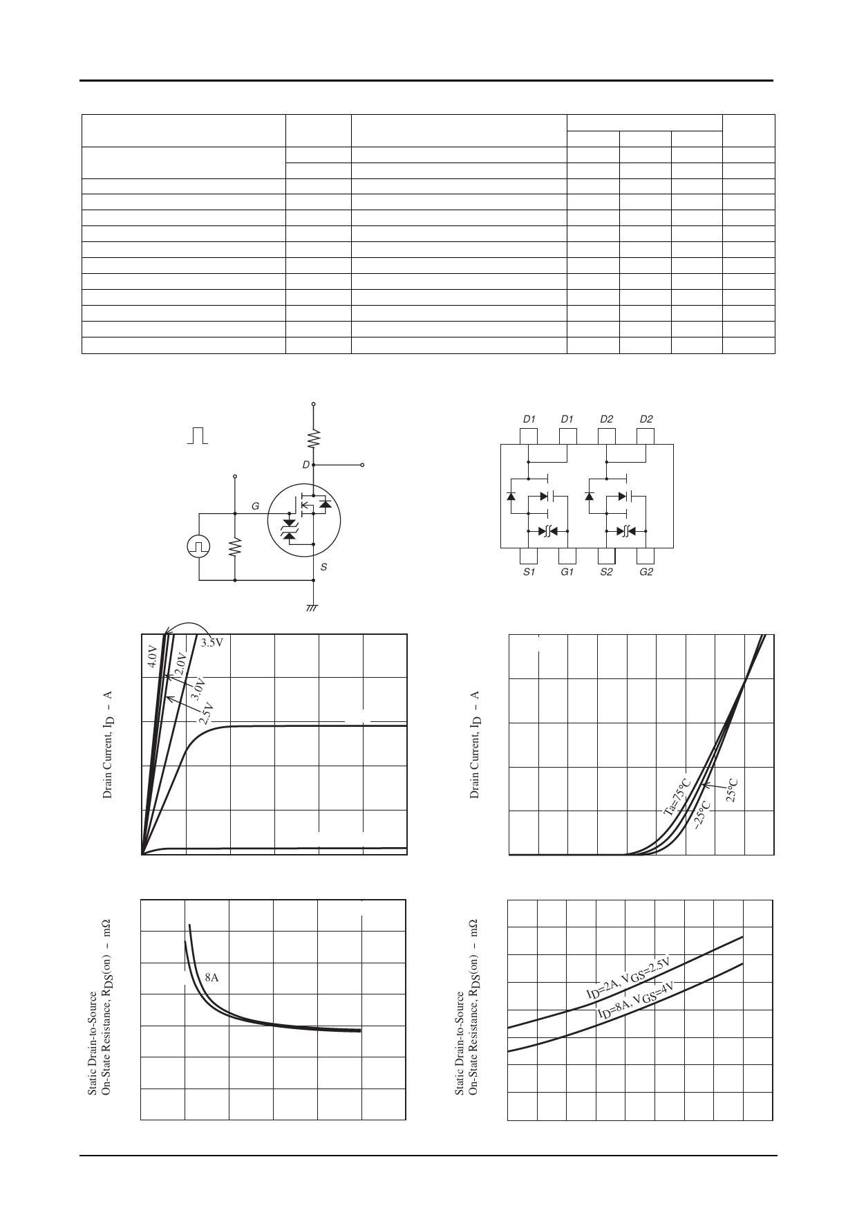
Switching Time Test Circuit
VIN
4V
0V
PW=10µs
D.C.≤1%
VIN
G
VDD=15V
ID=8A
RL=1.875Ω
D
VOUT
Electrical Connection
D1
D1
D2
D2
P.G
50Ω
FW232
S
S1 G1 S2
G2
(Top view)
ID -- VDS
15
3.5V
12
1.5V
9
6
3
VGS=1.0V
0
0
0.5
1.0
1.5
2.0
2.5
3.0
Drain-to-Source Voltage, VDS -- V IT02209
35
RDS(on) -- VGS
Ta=25°C
30
25
ID=2A 8A
20
15
10
5
0
0
2
4
6
8
10
12
Gate-to-Source Voltage, VGS -- V IT02211
15
VDS=10V
12
ID -- VGS
9
6
3
0
0 0.2 0.4 0.6 0.8 1.0 1.2 1.4 1.6 1.8
Gate-to-Source Voltage, VGS -- V IT02210
RDS(on) -- Ta
40
35
30
25
20
I DI=D2=A8, AV,GVSG=2S.=54VV
15
10
5
0
--50 --25
0
25 50 75 100 125 150 175
Ambient Temperature, Ta -- °C
IT02212
No.6618-2/4
Share Link: 