FW231 Просмотр технического описания (PDF) - SANYO -> Panasonic
Номер в каталоге
Компоненты Описание
производитель
FW231 Datasheet PDF : 4 Pages
| |||
FW231
Continued from preceding page.
Parameter
Input Capacitance
Output Capacitance
Reverse Transfer Capacitance
Turn-ON Delay Time
Rise Time
Turn-OFF Delay Time
Fall Time
Total Gate Charge
Gate-to-Source Charge
Gate-to-Drain "Miller" Charge
Diode Forward Voltage
Symbol
Conditions
Ciss
Coss
Crss
td(on)
tr
td(off)
tf
Qg
Qgs
Qgd
VSD
VDS=10V, f=1MHz
VDS=10V, f=1MHz
VDS=10V, f=1MHz
See specified Test Circuit
See specified Test Circuit
See specified Test Circuit
See specified Test Circuit
VDS=10V, VGS=10V, ID=9A
VDS=10V, VGS=10V, ID=9A
VDS=10V, VGS=10V, ID=9A
IS=9A, VGS=0
Ratings
Unit
min typ max
1950
pF
550
pF
370
pF
24
ns
440
ns
200
ns
300
ns
60
nC
2.8
nC
10
nC
0.82
1.2 V
Switching Time Test Circuit
4V VIN
0V
VIN
PW=10µs
D.C.≤1%
VDD=10V
ID=9A
RL=1.1Ω
D
VOUT
Electrical Connection
D1 D1 D2 D2
8765
G
P.G
50Ω
S FW231
A11946
18
3.5V
3.0V
16
2.5V
14
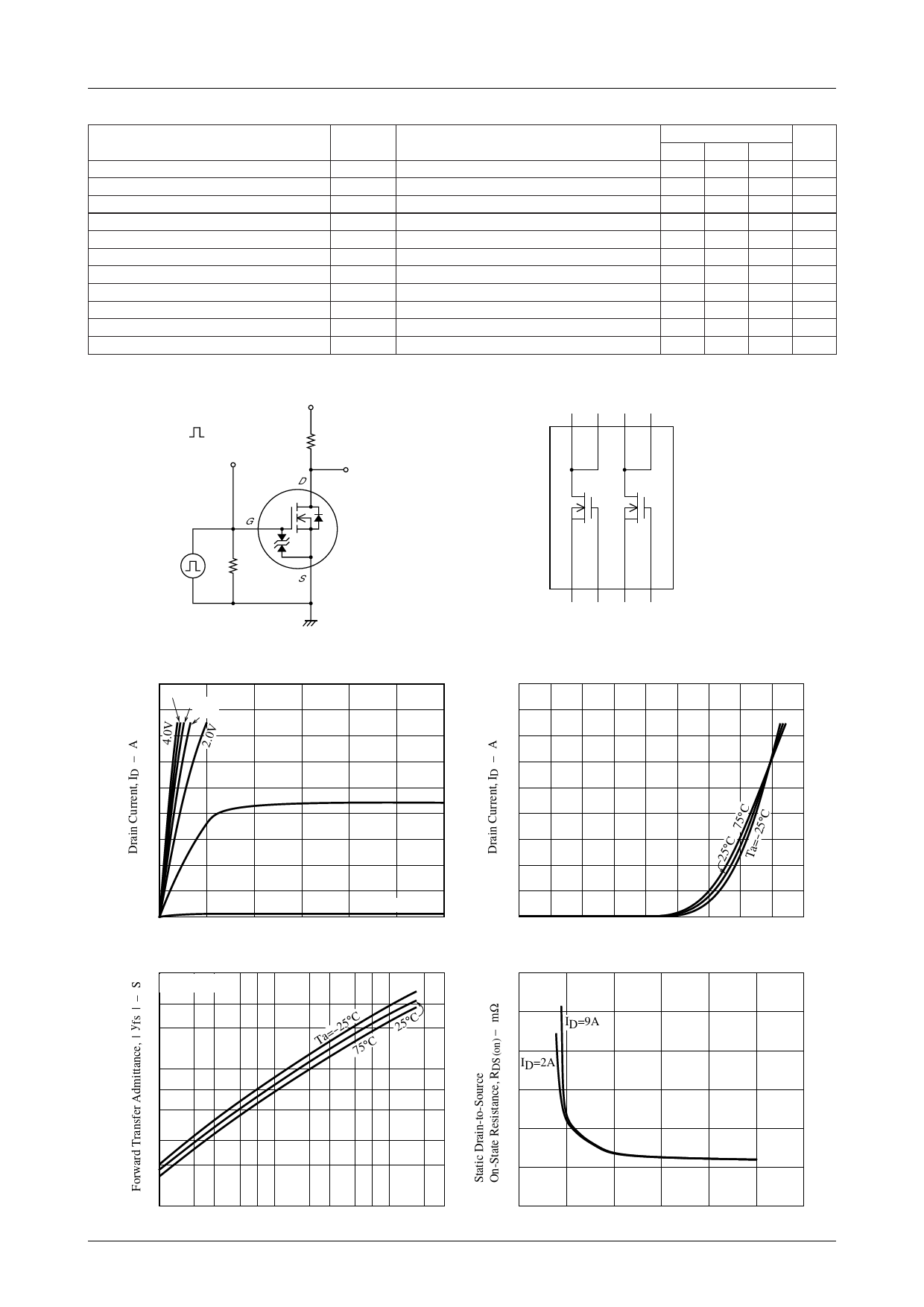
I D - VDS
12
10
1.5V
8
6
4
2
VGS=1.0V
00
0.5
1.0
1.5
2.0
2.5
3.0
Drain-to-Source Voltage, VDS – V
5
VDS=10V
| yfs | - I D
3
2
Ta=-25°C75°C
25°C
10
7
5
3
2
1.0
0.1
2 3 5 7 1.0
2 3 5 7 10
Drain Current, ID – A
23
1234
S1 G1 S2 G2
A12026
ID - VGS
18
16
14
12
10
8
6
4
2
0
0 0.2 0.4 0.6 0.8 1.0 1.2 1.4 1.6 1.8
Gate-to-Source Voltage, VGS – V
RDS(on) - VGS
60
Ta=25°C
50
ID=9A
40
ID=2A
30
20
10
00
2
4
6
8
10
12
Gate-to-Source Voltage, VGS – V
No.6071-2/4
Share Link: 