HFA1155 Просмотр технического описания (PDF) - Renesas Electronics
Номер в каталоге
Компоненты Описание
производитель
HFA1155 Datasheet PDF : 10 Pages
| |||
HFA1155
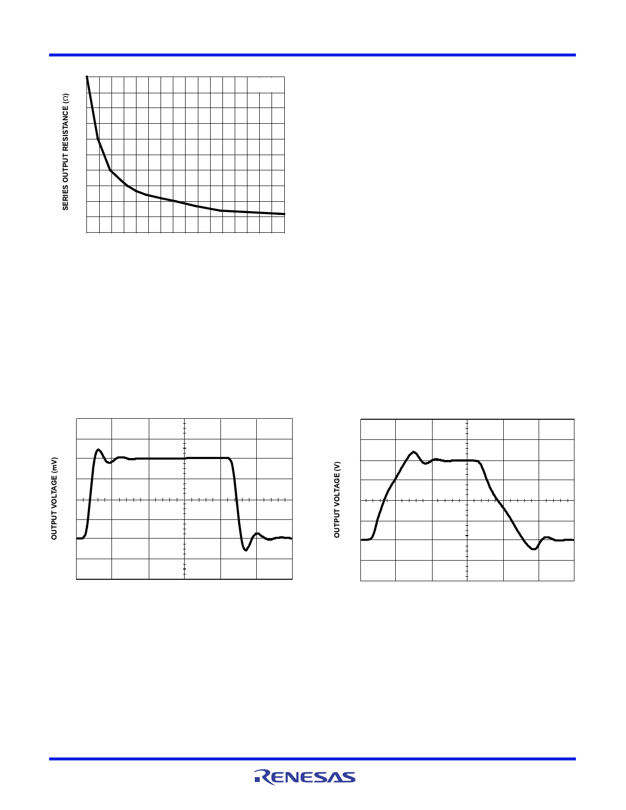
50
AV = +2
40
30
20
10
0
0
50 100 150 200 250 300 350 400
LOAD CAPACITANCE (pF)
FIGURE 1. RECOMMENDED SERIES OUTPUT RESISTOR vs
LOAD CAPACITANCE
PC Board Layout
The frequency response of this amplifier depends greatly on
the amount of care taken in designing the PC board. The use
of low inductance components such as chip resistors and
chip capacitors is strongly recommended, while a solid
ground plane is a must!
Attention should be given to decoupling the power supplies. A
large value (10F) tantalum in parallel with a small value chip
(0.1F) capacitor works well in most cases.
Terminated microstrip signal lines are recommended at the
input and output of the device. Output capacitance, such as
that resulting from an improperly terminated transmission line,
will degrade the frequency response of the amplifier and may
cause oscillations. In most cases, the oscillation can be
avoided by placing a resistor in series with the output.
Care must also be taken to minimize the capacitance to ground
seen by the amplifier’s inverting input. The larger this capacitance,
the worse the gain peaking, resulting in pulse overshoot and
eventual instability. To reduce this capacitance, remove the
ground plane under traces connected to -IN and keep these
traces as short as possible.
Typical Performance Curves VSUPPLY = 5V, RF = Value From the “Optimum Feedback Resistor” Table, TA = 25oC,
RL = 100, Unless Otherwise Specified
200
AV = +1
150
100
50
0
-50
-100
-150
-200
TIME (5ns/DIV.)
FIGURE 2. SMALL SIGNAL PULSE RESPONSE
2.0
AV = +1
1.5
1.0
0.5
0
-0.5
-1.0
-1.5
-2.0
TIME (5ns/DIV.)
FIGURE 3. LARGE SIGNAL PULSE RESPONSE
FN4863 Rev 1.00
September 2004
Page 5 of 10
Share Link: 