KGF1284 Просмотр технического описания (PDF) - Oki Electric Industry
Номер в каталоге
Компоненты Описание
производитель
KGF1284 Datasheet PDF : 7 Pages
| |||
¡ electronic components
KGF1284
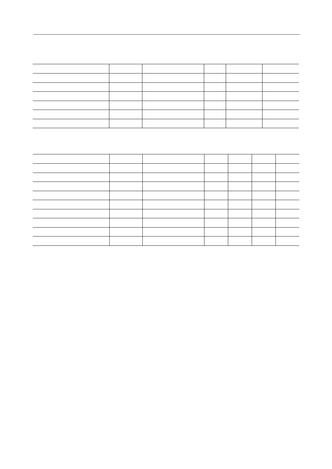
ABSOLUTE MAXIMUM RATINGS
Item
Drain-source voltage
Gate-source voltage
Drain current
Total power dissipation
Channel temperature
Storage temperature
Symbol
VDS
VGS
IDS
Ptot
Tch
Tstg
Condition
Ta = 25°C
Ta = 25°C
Ta = 25°C
Ta = Tc = 25°C
—
—
Unit
Min.
V
—
V
–5.0
A
—
W
—
°C
—
°C
–45
Max.
7.0
0.4
0.8
2.5
150
125
ELECTRICAL CHARACTERISTICS
Item
Gate-source leakage current
Gate-drain leakage current
Drain-source leakage current
Drain current
Gate-source cut-off voltage
Output power
Drain efficiency
Linear gain
Thermal resistance
Symbol
IGSS
IGDO
IDS(off)
IDSS
VGS(off)
PO
hD
GLIN
Rth
Condition
VGS = –5 V
VGD = –12 V
VDS = 7 V, VGS = –5 V
VDS = 1.5 V, VGS = 0 V
VDS = 3 V, IDS = 1.4 mA
(*1), PIN = 12 dBm
(*1), PIN = 12 dBm
(*1), PIN = –5 dBm
Channel to case
*1 Condition: f = 1.9 GHz, VDS = 3.4 V, IDSQ = 70 mA
Unit
mA
mA
mA
mA
V
dBm
%
dB
°C/W
Min.
—
—
—
450
–3.0
21.5
45
—
—
(Ta = 25°C)
Typ. Max.
—
50
—
150
—
500
—
—
—
–2.0
22.5
—
50
—
12.0
—
35
—
3/7
Share Link: 