ISL54405 Просмотр технического описания (PDF) - Renesas Electronics
Номер в каталоге
Компоненты Описание
производитель
ISL54405 Datasheet PDF : 20 Pages
| |||
ISL54405
Electrical Specifications 3.3V Supply: VDD = +3.0V to +3.6V, GND = 0V, VDIR_SEL = VAC/DC = GND, V5V_SUPPLY = Float,
VSIGNAL = 2VRMS, RLOAD = 20kΩ , f = 1kHz, VSELH = VMUTEH = 1.4V, VSELL = VMUTEL = 0.5V, CAP_SS = 0.1µF, (Note 10), Unless otherwise specified.
PARAMETER
TEST CONDITIONS
SUPPLY TEMP
MIN
MAX
(V) (°C) (Notes 11, 12) TYP (Notes 11, 12) UNITS
Input Voltage High, VSELH,
VMUTEH
3.3, Full
1.4
-
5
-
V
Input Current, ISELH, ISELL VDD = 3.6V, VMUTE = 0V, VSEL = 0V or VDD
3.6 Full
-0.5
0.01
0.5
µA
Input Current, IAC/DCL,
VDD = 3.6V, VAC/DC, VDIR_SEL = 0V, VMUTE = Float,
3.6 Full
-1.3
-0.7
0.3
µA
IDIR_SELL
VSEL = VDD
Input Current, IAC/DCH,
VDD = 3.6V, VAC/DC, VDIR_SEL = VDD, VMUTE = 0V,
3.6 Full
-0.5
0.01
0.5
µA
IDIR_SELH
VSEL = 0V
Input Current, IMUTEL
VDD = 3.6V, VSEL = VDD, VMUTE = 0V
3.6 Full
-1.3
-0.7
0.3
µA
Input Current, IMUTEH
VDD = 3.6V, VSEL = 0V, VMUTE = VDD
3.6 Full
-0.5
0.01
0.5
µA
NOTES:
10. VIN = input voltage to perform proper function.
11. The algebraic convention, whereby the most negative value is a minimum and the most positive a maximum, is used in this data sheet.
12. Parameters with MIN and/or MAX limits are 100% tested at +25°C, unless otherwise specified. Temperature limits established by characterization
and are not production tested.
13. Flatness is defined as the difference between maximum and minimum value of ON-resistance at the specified analog signal voltage points.
14. Limits established by characterization and are not production tested.
15. rON matching between channels is calculated by subtracting the channel with the highest max rON value from the channel with lowest max rON value.
16. Crosstalk is inversely proportional to source impedance.
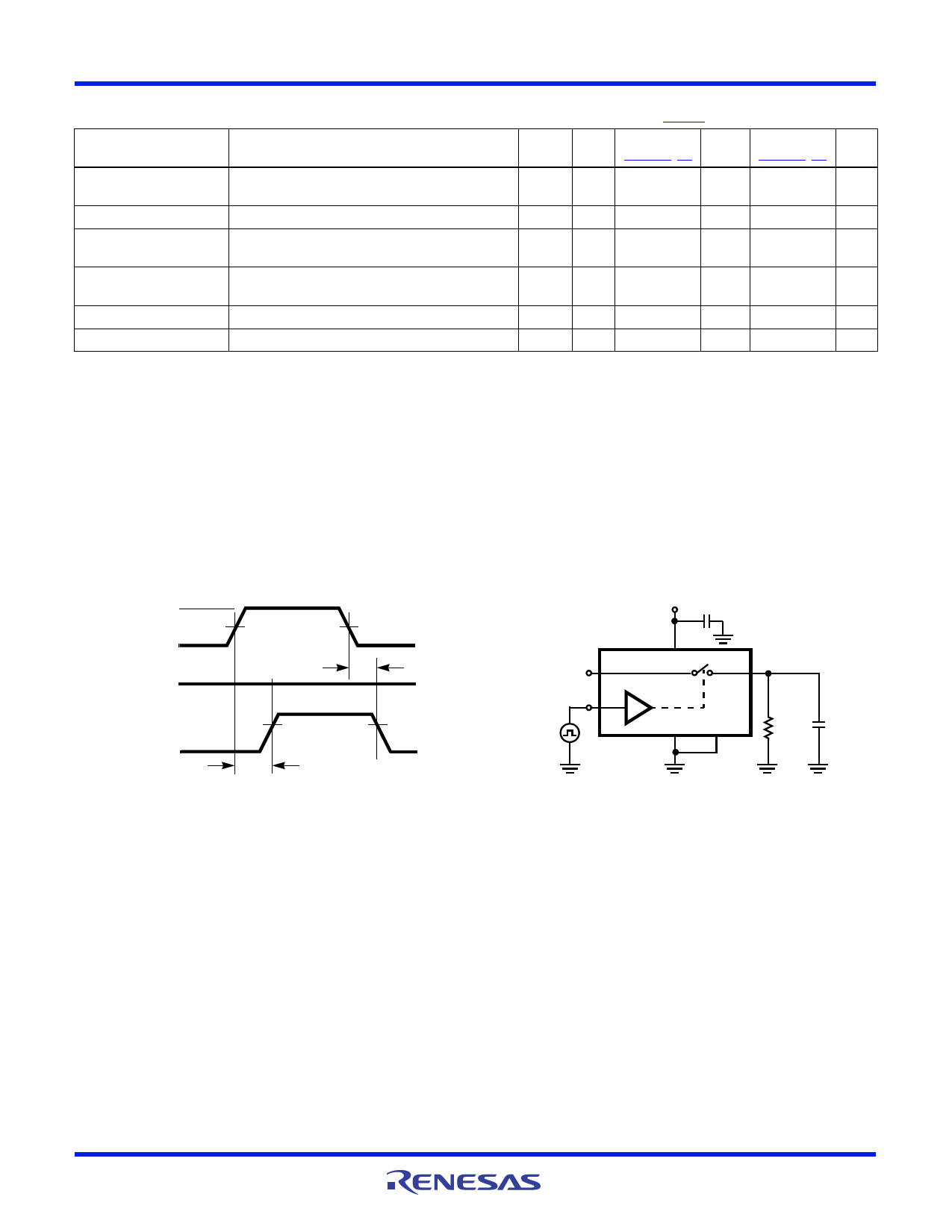
Test Circuits and Waveforms
VDD
LOGIC
INPUT
0V
SWITCH
INPUT
VLx OR VRx
SWITCH
OUTPUT 0V
50%
tOFF
VOUT
90%
tON
tr < 20ns
tf < 20ns
90%
Logic input waveform is inverted for switches that have the opposite logic
sense.
VDD C
SWITCH
INPUT
LOGIC
INPUT
Lx OR Rx
SEL
L or R
GND MUTE
VOUT
RL
CL
Repeat test for all switches. CL includes fixture and stray
capacitance.
VOUT = V(Lx or Rx) R-----L----R+-----Lr---O----N--
FIGURE 2A. MEASUREMENT POINTS
FIGURE 2. SWITCHING TIMES
FIGURE 2B. TEST CIRCUIT
FN6699 Rev 2.00
May 6, 2014
Page 6 of 20
Share Link: 