MJD41C Просмотр технического описания (PDF) - ON Semiconductor
Номер в каталоге
Компоненты Описание
производитель
MJD41C Datasheet PDF : 7 Pages
| |||
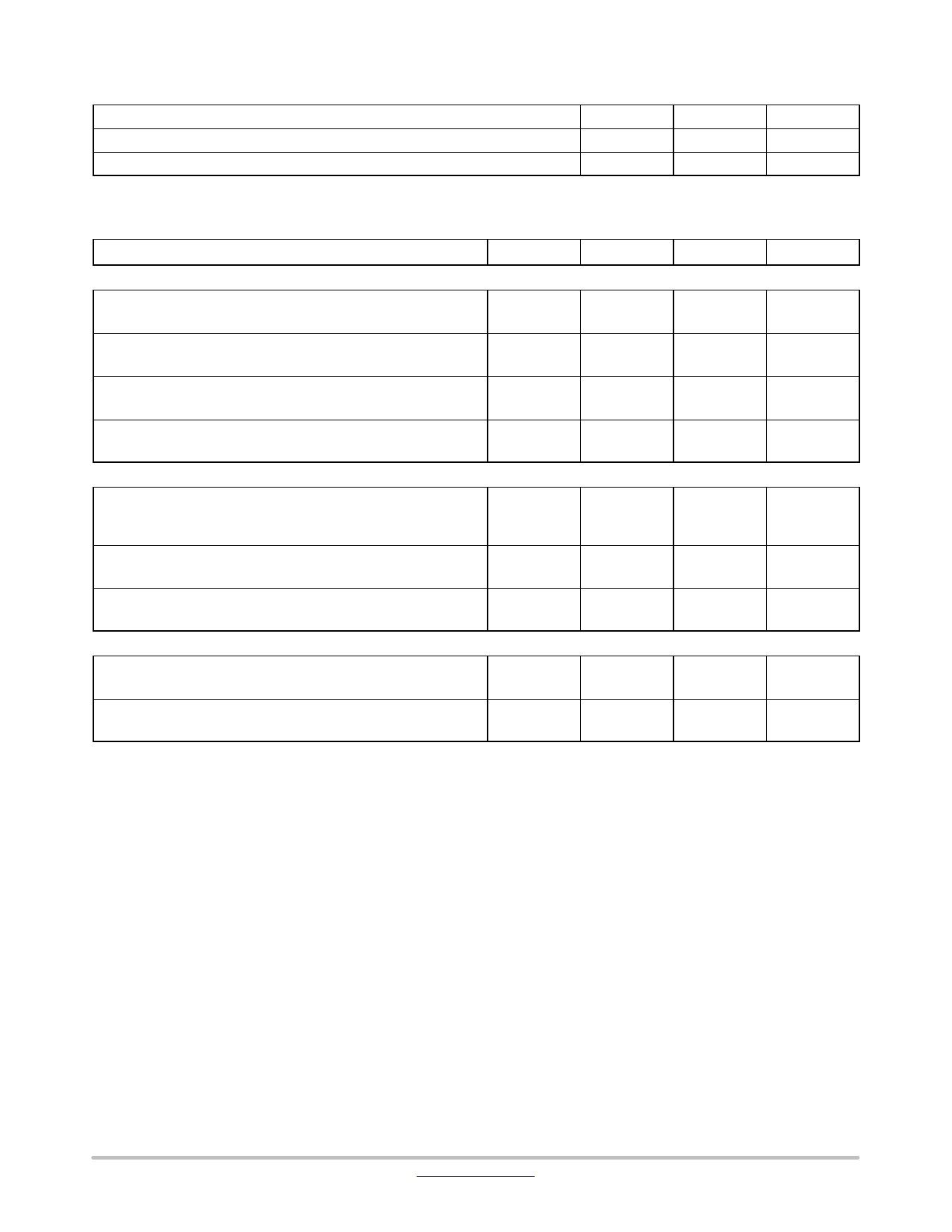
MJD41C (NPN), MJD42C (PNP)
THERMAL CHARACTERISTICS
Characteristic
Symbol
Max
Thermal Resistance, Junction−to−Case
RqJC
6.25
Thermal Resistance, Junction−to−Ambient (Note 2)
RqJA
71.4
2. These ratings are applicable when surface mounted on the minimum pad sizes recommended.
Unit
°C/W
°C/W
ELECTRICAL CHARACTERISTICS (TC = 25_C unless otherwise noted)
Characteristic
Symbol
Min
Max
Unit
OFF CHARACTERISTICS
Collector−Emitter Sustaining Voltage (Note 3)
(IC = 30 mAdc, IB = 0)
VCEO(sus)
Vdc
100
−
Collector Cutoff Current
(VCE = 60 Vdc, IB = 0)
ICEO
−
mAdc
50
Collector Cutoff Current
(VCE = 100 Vdc, VEB = 0)
ICES
−
mAdc
10
Emitter Cutoff Current
(VBE = 5 Vdc, IC = 0)
IEBO
−
mAdc
0.5
ON CHARACTERISTICS (Note 3)
DC Current Gain
(IC = 0.3 Adc, VCE = 4 Vdc)
(IC = 3 Adc, VCE = 4 Vdc)
hFE
−
30
−
15
75
Collector−Emitter Saturation Voltage
(IC = 6 Adc, IB = 600 mAdc)
VCE(sat)
−
Vdc
1.5
Base−Emitter On Voltage
(IC = 6 Adc, VCE = 4 Vdc)
VBE(on)
−
Vdc
2
DYNAMIC CHARACTERISTICS
Current Gain − Bandwidth Product (Note 4)
(IC = 500 mAdc, VCE = 10 Vdc, ftest = 1 MHz)
fT
MHz
3
−
Small−Signal Current Gain
(IC = 0.5 Adc, VCE = 10 Vdc, f = 1 kHz)
hfe
−
20
−
Product parametric performance is indicated in the Electrical Characteristics for the listed test conditions, unless otherwise noted. Product
performance may not be indicated by the Electrical Characteristics if operated under different conditions.
3. Pulse Test: Pulse Width ≤ 300 ms, Duty Cycle ≤ 2%.
4. fT = ⎪hfe⎪• ftest.
www.onsemi.com
2
Share Link: 