ISL6446A –Я—А–Њ—Б–Љ–Њ—В—А —В–µ—Е–љ–Є—З–µ—Б–Ї–Њ–≥–Њ –Њ–њ–Є—Б–∞–љ–Є—П (PDF) - Renesas Electronics
–Э–Њ–Љ–µ—А –≤ –Ї–∞—В–∞–ї–Њ–≥–µ
–Ъ–Њ–Љ–њ–Њ–љ–µ–љ—В—Л –Ю–њ–Є—Б–∞–љ–Є–µ
–њ—А–Њ–Є–Ј–≤–Њ–і–Є—В–µ–ї—М
ISL6446A Datasheet PDF : 22 Pages
| |||
ISL6446A
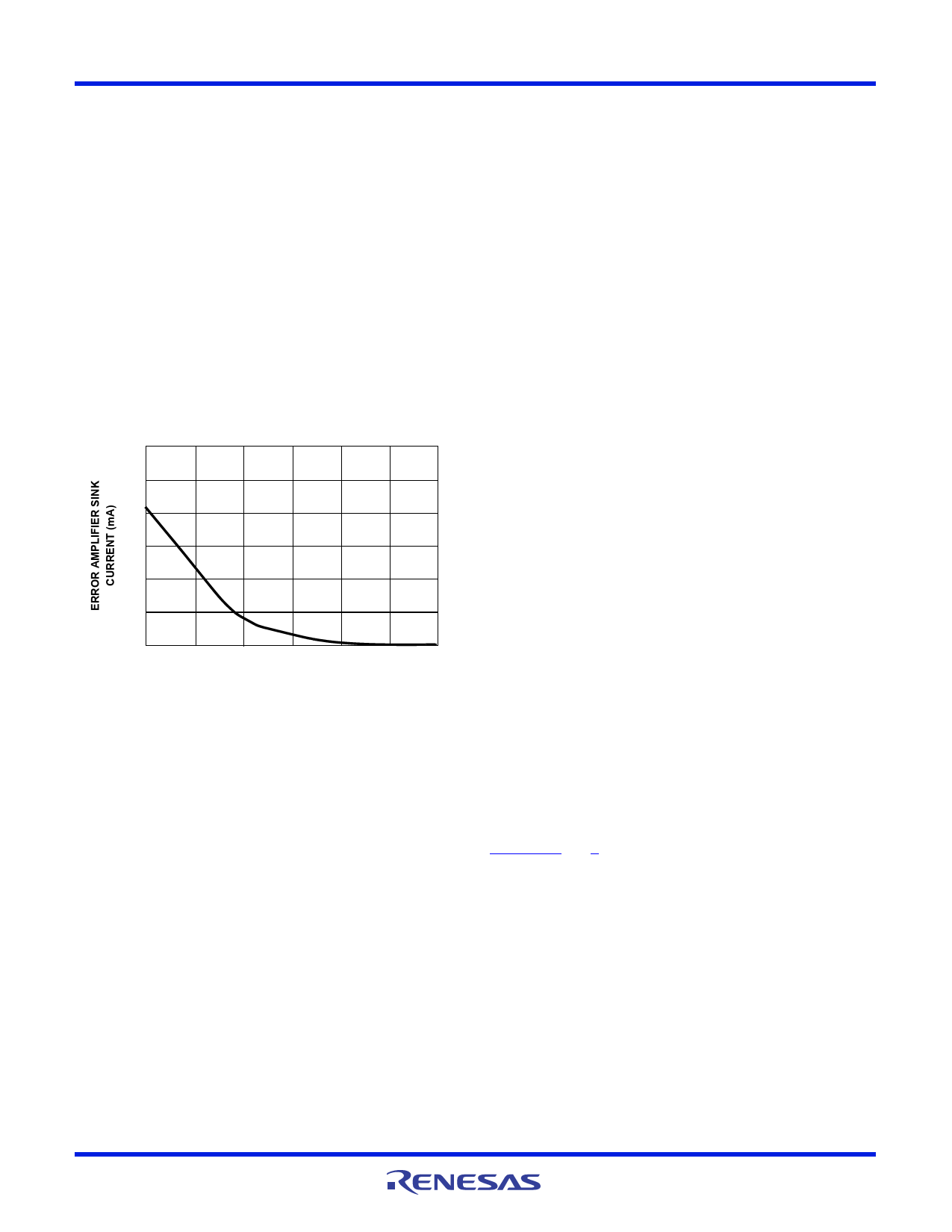
Linear Regulator
The linear regulator controller is a transconductance amplifier
with a nominal gain of 2A/V. The N-channel MOSFET output
buffer can sink a minimum of 50mA.
The reference voltage is 0.6V. With 0V differential at its input, the
controller sinks 21mA of current. For better load regulation, it is
recommended that the resistor from the LDO input to the base of
the PNP (or gate of the PFET) is set so that the sink current at G4
pin is within 9mA to 31mA over the entire load and temperature
range.
An external PNP transistor or P-channel MOSFET pass device can
be used. The dominant pole for the loop can be placed at the
base of the PNP (or gate of the PFET), as a capacitor from
emitter-to-base (source to gate of a PFET). Better load transient
response is achieved however, if the dominant pole is placed at
the output with a capacitor to ground at the output of the
regulator.
60
50
40
30
20
10
0
0.59
0.6
0.61
0.62
0.63
0.64
0.65
FEEDBACK VOLTAGE (V)
FIGURE 24. LINEAR CONTROLLER GAIN
Protection Mechanisms
OCP- (Function independent for both PWM). The overcurrent
function protects the PWM converter from a shorted output by
using the upper MOSFETвАЩs ON-resistance, rDS(ON) to monitor the
current. This method enhances the converterвАЩs efficiency and
reduces cost by eliminating a current sensing resistor. The
overcurrent function latches off the outputs to provide fault
protection. A resistor connected to the drain of the upper MOSFET
and OCSET pin programs the overcurrent trip level. The PHASE
node voltage will be compared against the voltage on the OCSET
pin, while the upper MOSFET is on. A current (typically 110µA) is
pulled from the OCSET pin to establish the OCSET voltage. If
PHASE is lower than OCSET while the upper MOSFET is on, then
an overcurrent condition is detected for that clock cycle. The
upper gate pulse is immediately terminated, and a counter is
incremented. If an overcurrent condition is detected for 32
consecutive clock cycles, the ISL6446A output is latched off with
gate drivers three-stated. The switcher will restart when the
SS/EN pin is externally driven below 1V, or if power is recycled to
the chip. During soft-start, both pulse termination current limiting
and the 32-cycle counter are enabled.
UVP - (Function independent for both PWM). If the voltage on the
FB pin falls to 82% (typical) of the reference voltage for 8
FN8384 Rev 3.00
Aug 27, 2015
consecutive PWM cycles, then the circuit enters into soft-start
hiccup mode. During hiccup, the external capacitor on the SS/EN
pin is discharged, then released and a soft-start cycle is initiated.
The UVP comparator is separate from the one sensing for
PGOOD, which should have already detected a problem, before
the UVP trips.
OVP - (Function independent for both PWM). The OVP function is
enabled after the soft-start has finished. If voltage on the FB pin
rises to 116% (typical) of the reference voltage, the lower gate
driver is turned on continuously. If the overvoltage condition
continues for 32 consecutive PWM cycles, then the output is
latched off with the gate drivers three-stated. The capacitor on the
SS/EN pin will not be discharged. The switcher will restart when
the SS/EN pin is externally driven below 1V, or if power is recycled
to the chip. The OVP comparator is separate from the one sensing
for PGOOD, which should have already detected a problem
before the OVP trips.
Application Guidelines
PWM Controller
DISCUSSION
The PWM must be compensated such that it achieves the
desired transient performance goals, stability and DC regulation
requirements.
The first parameter that needs to be chosen is the switching
frequency, fSW. This decision is based on the overall size
constraints and the frequency plan of the end equipment.
Smaller space requires higher frequency. This allows the output
inductor, input capacitor bank, and output capacitor bank to be
reduced in size and/or value. The power supply must be designed
such that the frequency and its distribution over component
tolerance, time and temperature causes minimal interference in
RF stages, IF stages, PLL loops, mixers, etc.
INDUCTOR SELECTION
The output inductor is selected to meet the output voltage ripple
requirements and minimize the converterвАЩs response time to the
load transient. The inductor value determines the converterвАЩs
ripple current, and the ripple voltage is a function of the ripple
current. The ripple current and voltage are approximated by
Equations 7 and 8, where ESR is the output capacitance ESR
value.
пБДI = -V----I--Nf--S-----W----V--пВЈ--O--L--U-----T- пВЈ V----V-O---I-U-N---T--
(EQ. 7)
пБДVOUT = пБДI x ESR
(EQ. 8)
Increasing the value of inductance reduces the ripple current and
voltage. However, the large inductance value reduces the
converterвАЩs response time to a load transient (and usually
increases the DCR of the inductor, which decreases the
efficiency). Increasing the switching frequency (fSW) for a given
inductor also reduces the ripple current and voltage.
One of the parameters limiting the converterвАЩs response to a load
transient is the time required to change the inductor current.
Page 15 of 22
Share Link: 