ADA4857-2YCPZ-R7 Просмотр технического описания (PDF) - Analog Devices
Номер в каталоге
Компоненты Описание
производитель
ADA4857-2YCPZ-R7 Datasheet PDF : 21 Pages
| |||
Data Sheet
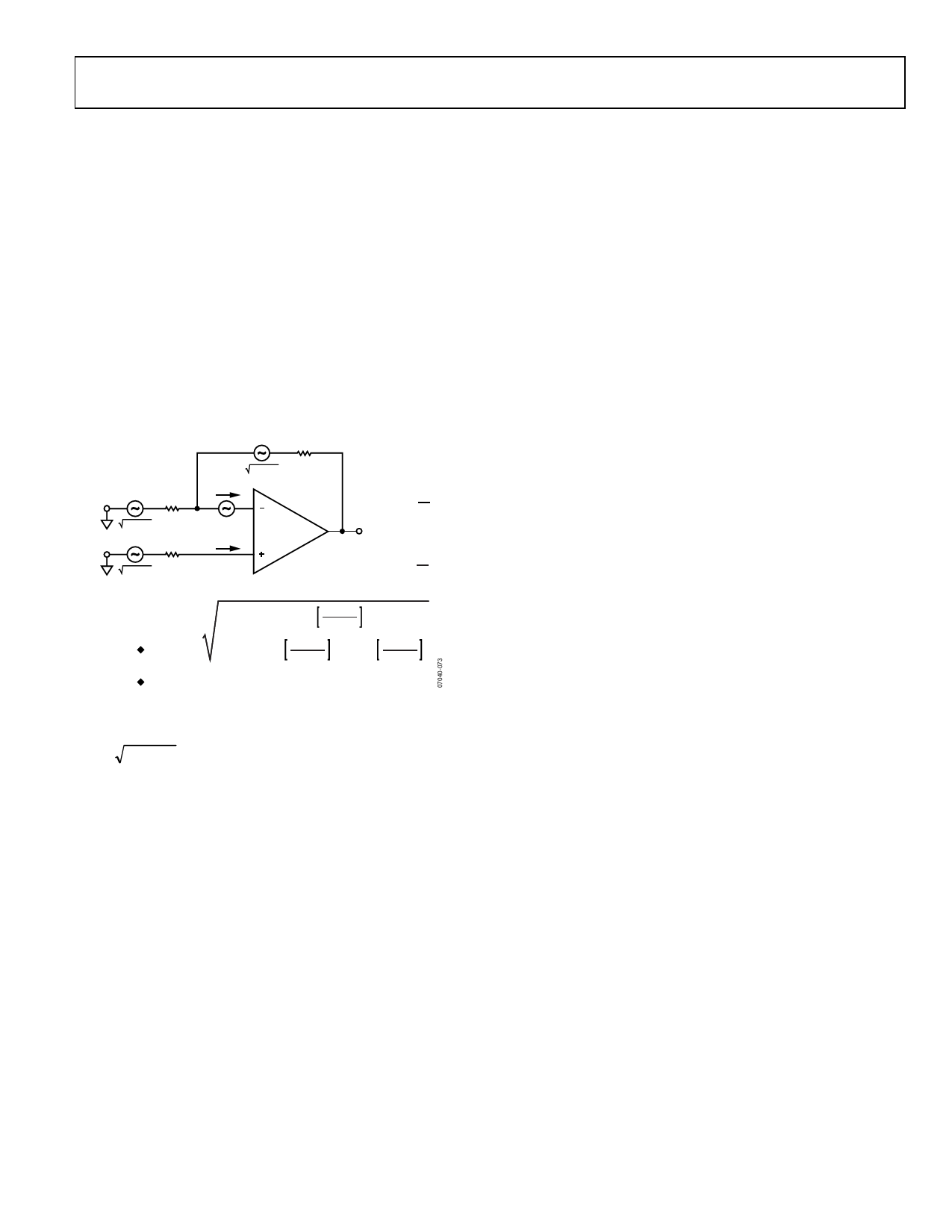
NOISE
To analyze the noise performance of an amplifier circuit, identify
the noise sources and determine if the source has a significant
contribution to the overall noise performance of the amplifier.
To simplify the noise calculations, noise spectral densities were
used rather than actual voltages to leave bandwidth out of the
expressions (noise spectral density, which is generally expressed
in nV/Hz, is equivalent to the noise in a 1 Hz bandwidth).
The noise model shown in Figure 57 has six individual noise
sources: the Johnson noise of the three resistors, the operational
amplifier voltage noise, and the current noise in each input of the
amplifier. Each noise source has its own contribution to the noise
at the output. Noise is generally referred to input (RTI), but it is
often easier to calculate the noise referred to the output (RTO)
and then divide by the noise gain to obtain the RTI noise.
VN, R2
R2
4kTR2
GAIN FROM
A TO OUTPUT
=
B VN, R1
R1
IN–
4kTR1
VN
A VN, R3
R3
IN+
4kTR3
NOISE GAIN =
NG
=
1
+
R2
R1
VOUT
GAIN FROM
B TO OUTPUT
=
–
R2
R1
RTI NOISE =
VN2 + 4kTR3 + 4kTR1
R2
R1 + R2
2
+IN+2R32 + IN–2
R1 × R2
R1 + R2
2
+ 4kTR2
R1
R1 + R2
2
RTO NOISE = NG × RTI NOISE
Figure 57. Operational Amplifier Noise Analysis Model
All resistors have Johnson noise that is calculated by
(4kBTR)
where:
k is Boltzmann’s Constant (1.38 × 10⁻²³ J/K).
B is the bandwidth in Hertz.
T is the absolute temperature in Kelvin.
R is the resistance in ohms.
A simple relationship that is easy to remember is that a 50 Ω
resistor generates a Johnson noise of 1 nV/Hz at 25°C.
In applications where noise sensitivity is critical, care must
be taken not to introduce other significant noise sources to
the amplifier. Each resistor is a noise source. Attention to the
following areas is critical to maintain low noise performance:
design, layout, and component selection. A summary of noise
performance for the amplifier and associated resistors can be
seen in Table 9.
ADA4857-1/ADA4857-2
CIRCUIT CONSIDERATIONS
Careful and deliberate attention to detail when laying out the
ADA4857 board yields optimal performance. Power supply
bypassing, parasitic capacitance, and component selection all
contribute to the overall performance of the amplifier.
PCB LAYOUT
Because the ADA4857 can operate up to 850 MHz, it is essential
that RF board layout techniques be employed. All ground and
power planes under the pins of the ADA4857 must be cleared of
copper to prevent the formation of parasitic capacitance between
the input pins to ground and the output pins to ground. A single
mounting pad on the SOIC footprint can add as much as 0.2 pF
of capacitance to ground if the ground plane is not cleared from
under the mounting pads. The low distortion pinout of the
ADA4857 increases the separation distance between the inputs
and the supply pins, which improves the second harmonics. In
addition, the feedback pin reduces the distance between the output
and the inverting input of the amplifier, which helps minimize
the parasitic inductance and capacitance of the feedback path,
reducing ringing and peaking.
POWER SUPPLY BYPASSING
Power supply bypassing for the ADA4857 was optimized for
frequency response and distortion performance. Figure 49 shows
the recommended values and location of the bypass capacitors. The
0.1 μF bypassing capacitors must be placed as close as possible to
the supply pins. Power supply bypassing is critical for stability,
frequency response, distortion, and PSR performance. The
capacitor between the two supplies helps improve PSR and
distortion performance. The 10 μF electrolytic capacitors must be
close to the 0.1 μF capacitors; however, it is not as critical. In some
cases, additional paralleled capacitors can help improve frequency
and transient response.
GROUNDING
Ground and power planes must be used where possible. Ground
and power planes reduce the resistance and inductance of the
power planes and ground returns. The returns for the input, output
terminations, bypass capacitors, and RG must all be kept as close to
the ADA4857 as possible. The output load ground and the bypass
capacitor grounds must be returned to the same point on the
ground plane to minimize parasitic trace inductance, ringing, and
overshoot and to improve distortion performance. The ADA4857
LFSCP packages feature an exposed paddle. For optimum electrical
and thermal performance, solder this paddle to the ground plane
or the power plane. For more information on high speed circuit
design, see A Practical Guide to High-Speed Printed-Circuit-
Board Layout at www.analog.com.
Rev. D | Page 19 of 21
Share Link: 