MTD6N10E Просмотр технического описания (PDF) - ON Semiconductor
Номер в каталоге
Компоненты Описание
производитель
MTD6N10E Datasheet PDF : 10 Pages
| |||
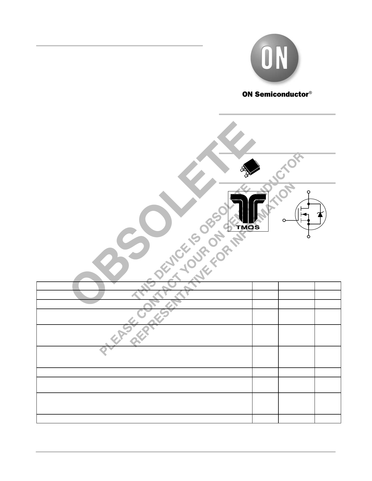
MTD6N10E
Designer’s™ Data Sheet
TMOS E−FET.™
Power Field Effect
Transistor
DPAK for Surface Mount
N−Channel Enhancement−Mode Silicon
Gate
This advanced TMOS E−FET is designed to withstand high energy
in the avalanche and commutation modes. The new energy efficient
design also offers a drain−to−source diode with a fast recovery time.
Designed for low voltage, high speed switching applications in power
supplies, converters and PWM motor controls, these devices are
particularly well suited for bridge circuits where diode speed and
commutating safe operating areas are critical and offer additional
safety margin against unexpected voltage transients.
• Avalanche Energy Specified
• Source−to−Drain Diode Recovery Time Comparable to a Discrete
Fast Recovery Diode
• Diode is Characterized for Use in Bridge Circuits
• IDSS and VDS(on) Specified at Elevated Temperature
• Surface Mount Package Available in 16 mm, 13−inch/2500
Unit Tape & Reel, Add T4 Suffix to Part Number
• Replaces MTD5N10
http://onsemi.com
TMOS POWER FET
6.0 AMPERES, 100 VOLTS
RDS(on) = 0.400 W
DPAK
CASE 369A−13
Style 2
D
®
G
S
MAXIMUM RATINGS (TC = 25°C unless otherwise noted)
Rating
Symbol
Value
Unit
Drain−Source Voltage
Drain−Gate Voltage (RGS = 1.0 MΩ)
Gate−Source Voltage — Continuous
Gate−Source Voltage — Non−Repetitive (tp ≤ 10 ms)
VDSS
100
Vdc
VDGR
100
Vdc
VGS
± 20
Vdc
VGSM
± 40
Vpk
Drain Current — Continuous
Drain Current — Continuous @ 100°C
Drain Current — Single Pulse (tp ≤ 10 μs)
ID
6.0
Adc
ID
4.5
IDM
18
Apk
Total Power Dissipation
Derate above 25°C
Total Power Dissipation @ TA = 25°C, when mounted to minimum recommended pad size
PD
40
Watts
0.32
W/°C
1.75
Watts
Operating and Storage Temperature Range
TJ, Tstg
−55 to 150
°C
Single Pulse Drain−to−Source Avalanche Energy — Starting TJ = 25°C
(VDD = 25 Vdc, VGS = 10 Vdc, IL = 6.0 Apk, L = 3.0 mH, RG =25 Ω)
EAS
50
mJ
Thermal Resistance — Junction to Case
Thermal Resistance — Junction to Ambient
Thermal Resistance — Junction to Ambient, when mounted to minimum recommended pad size
RθJC
RθJA
RθJA
3.13
°C/W
100
71.4
Maximum Temperature for Soldering Purposes, 1/8″ from case for 10 seconds
TL
260
°C
Designer’s Data for “Worst Case” Conditions — The Designer’s Data Sheet permits the design of most circuits entirely from the information presented. SOA Limit
curves — representing boundaries on device characteristics — are given to facilitate “worst case” design.
Preferred devices are Motorola recommended choices for future use and best overall value.
© Semiconductor Components Industries, LLC, 2006
1
August, 2006 − Rev. 3
Publication Order Number:
MTD6N10E/D
Share Link: 