UPD78C11AGF(A)-XXX-3BE Просмотр технического описания (PDF) - NEC => Renesas Technology
Номер в каталоге
Компоненты Описание
производитель
UPD78C11AGF(A)-XXX-3BE Datasheet PDF : 60 Pages
| |||
µPD78C10A(A), 78C11A(A), 78C12A(A)
2. DIFFERENCES BETWEEN (1) µPD78C10A(A) AND (2) µPD78C11A(A) AND 78C12A(A)
The main difference between the µPD78C10A(A) and the µPD78C11A(A) and 78C12A(A) is that the
µPD78C10A(A) does not have an on-chip mask programmable ROM. This results in the memory mapping
differences described below.
(1) µPD78C10A(A)
Because the µPD78C10A(A) does not have on-chip ROM, all memory except for the on-chip RAM area
(FF00H to FFFFH) are installed externally. The amount of externally installed memory can be set using
the MODE0 and MODE1 pins. As shown in the following table and in Figure 2-1, there are three memory
access options: 4 Kbytes (0000H to 0FFFH), 16 Kbytes (0000H to 3FFFH) and 64 Kbytes (0000H to FEFFH).
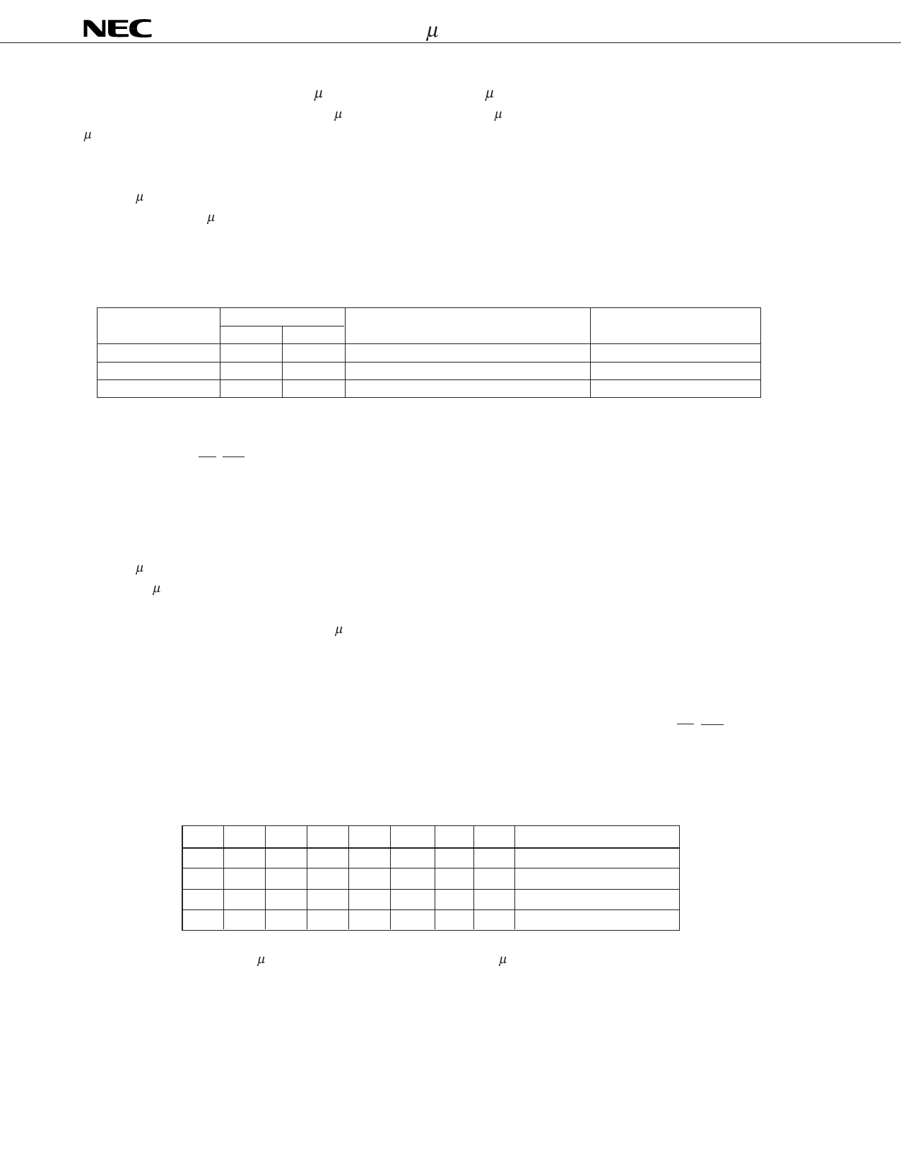
Operation mode
4-Kbyte access
16-Kbyte access
64-Kbyte access
Control pins
MODE1 MODE0
0
0
0
1
1
1
External memory
4 Kbytes (addresses 0000H to 0FFFH)
16 Kbytes (addresses 0000H to 3FFFH)
64 Kbytes (addresses 0000H to FEFFH)
On-chip RAM
Addresses FF00H to FFFFH
Addresses FF00H to FFFFH
Addresses FF00H to FFFFH
External memory can be accessed via PD0 to PD7 (multiplexed address/data buses), PF0 to PF7 (address
buses), or the RD, WR, or ALE signals. When accessing 4 Kbytes or 16 Kbytes of external memory, address
buses (PF0 to PF7) that are not being used as address lines can be used as an ordinary I/O port.
Use the MODE0 and MODE1 pins to select the amount of externally installed memory and set the
memory mapping register’s MM2, MM1, and MM0 bits to “0”.
(2) µPD78C11A(A), 78C12A(A)
The µPD78C11A(A) has on-chip mask programmable ROM from addresses 0000H to 0FFFH and on-chip
RAM from addresses FF00H to FFFFH. Up to 60 Kbytes (addresses 1000H to FEFFH) of external expansion
memory can be added in steps. The µPD78C12A(A) has on-chip mask programmable ROM from addresses
0000H to 1FFFH and on-chip RAM from addresses FF00H to FFFFH. Up to 56 Kbytes (addresses 2000H
to FEFFH) of external expansion memory can be added in steps.
Set the memory mapping register to select among five external expansion memory modes: no external
memory, 256 bytes, 4 Kbytes, 16 Kbytes, and 56 or 60 Kbytes(Note). External memory can be accessed
via PD0 to PD7 (multiplexed address/data buses), PF0 to PF7 (address buses), or using the RD, WR, or ALE
signals. External memory can contain either programs or data. Some address buses (PF0 to PF7) are used
as address lines, depending on the memory size, and any remaining address buses can be used as an
ordinary I/O port.
PF7 PF6 PF5 PF4 PF3 PF2 PF1
Port Port Port Port Port Port Port
Port Port Port Port AB11 AB10 AB9
Port Port AB13 AB12 AB11 AB10 AB9
AB15 AB14 AB13 AB12 AB11 AB10 AB9
PF0
Port
AB8
AB8
AB8
External memory
256 bytes max
4 Kbytes max
16 Kbytes max
56/60 Kbytes max(Note)
Note 56 Kbytes for the µPD78C12A(A) and 60 Kbytes for the µPD78C11A(A)
16
Share Link: 