BR24A01AFJ-WM Просмотр технического описания (PDF) - ROHM Semiconductor
Номер в каталоге
Компоненты Описание
производитель
BR24A01AFJ-WM Datasheet PDF : 32 Pages
| |||
BR24Axxx-WM (1K 2K 4K 8K 16K 32K 64K)
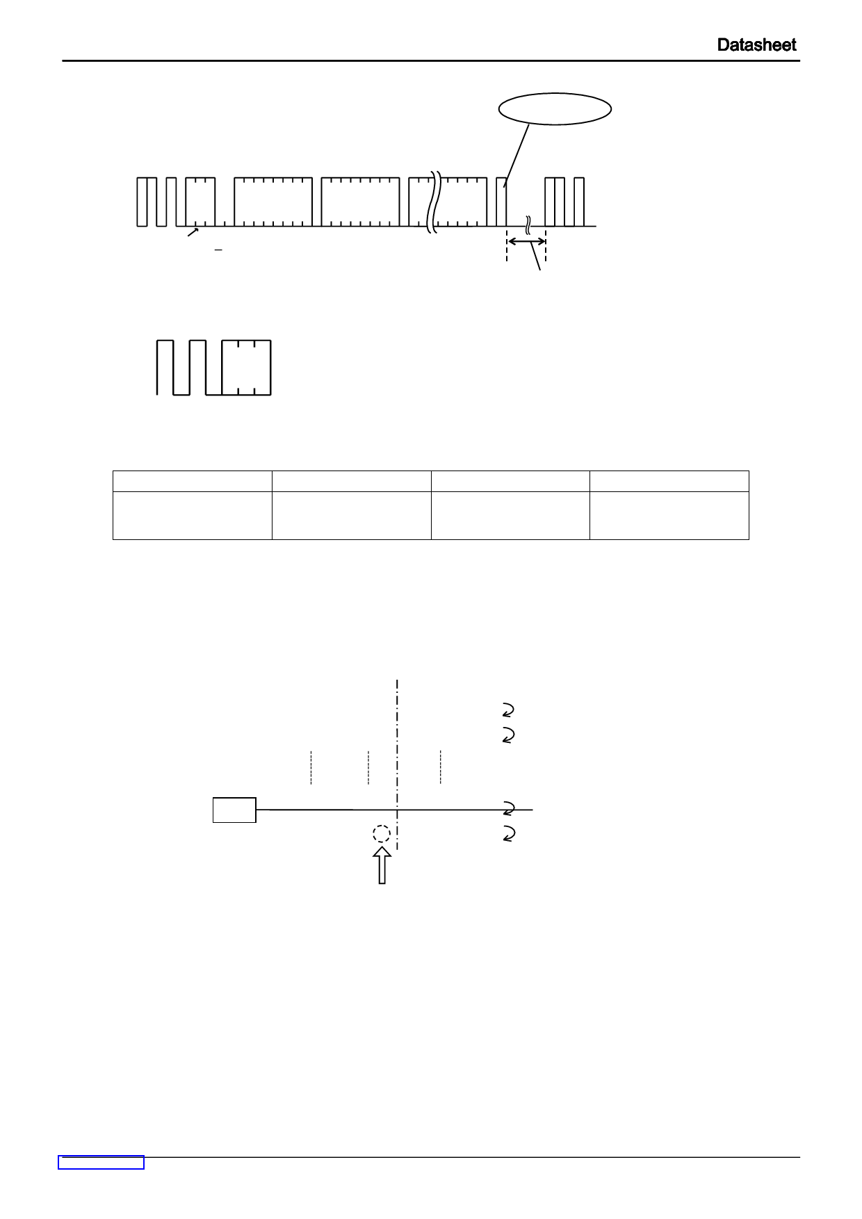
○Notes on write cycle continuous input
SDA
LINE
S
T
A
R
T
SLAVE
ADDRESS
W
R
I
T
E
WORD
ADDRESS(n)
DATA(n)
*1
1 0 1 0 A2A1A0 WA
7
00
RA
Note)
/C
WK
WA
0
D7
A
C
K
D0
A
C
K
S
T
DATA(n+7)**23
O
P
D0
A
C
K
At STOP (stop bit),
write starts.
S
T
A
R
T
1 0 10
00 00
Next command
Note)
Figure 39. Page write cycle
*1
*2
*3
tWR(maximum : 5ms)
Command is not accepted for this period.
BR24A01A-WM becomes Don’t care.
BR24A04-WM, BR24A08-W, and BR24A16-WM become (n+15).
BR24A32-WM and BR24A64-WM become (n+31).
*1 *2 *3
1 0 1 0 A2A1A0
00
Figure 40. Difference of each type of slave address
*1 In BR24A16-WM, A2 becomes P2.
*2 In BR24A08-WM, BR24A16-WM, A1 become P1.
*3 In BR24A04-WM, A0 becomes PS, and in
BR24A08-WM and in BR24A16-WM, A0 becomes P0.
○Notes on page write cycle
List of numbers of page write
Number of Pages
Product
number
8Byte
BR24A01A-WM
BR24A02-WM
16Byte
BR24A04-WM
BR24A08-WM
BR24A16-WM
32Byte
BR24A32-WM
BR24A64-WM
The above numbers are maximum bytes for respective types.
Any bytes below these can be written.
In the case BR24A02-WM, 1 page=8bytes, but the page write cycle write time is 5ms at maximum for 8byte bulk write.
It does not stand 5ms at maximum × 8byte=40ms(Max.).
○Internal address increment
Page write mode (in the case of BR24A02-WM)
WA7 ----- WA4 WA3
0 ----- 0
0
0 ----- 0
0
0 ----- 0
0
WA2
0
0
0
WA1
0
0
1
WA0
0
1
0
Increment
0 ----- 0
06h 0 ----- 0
0 ----- 0
0110
0111
0000
Significant bit is fixed.
No digit up
For example, when it is started from address 06h, therefore, increment is made as below,
06h → 07h → 00h → 01h ---, which please note.
*06h・・・06 in hexadecimal, therefore, 00000110 becomes a binary number.
○Write protect (WP) terminal
・Write protect (WP) function
When WP terminal is set VCC (H level), data rewrite of all addresses is prohibited. When it is set GND (L level), data rewrite of
all address is enabled. Be sure to connect this terminal to VCC or GND, or control it to H level or L level. Do not use it open.
At extremely low voltage at power ON / OFF, by setting the WP terminal 'H', mistake write can be prevented.
During tWR, set the WP terminal always to 'L'. If it is set 'H', write is forcibly terminated.
www.rohm.com
© 2012 ROHM Co., Ltd. All rights reserved.
TSZ22111・15・001
15/28
TSZ02201-0R1R0G100140-1-2
29.Jan.2018 Rev.003
Share Link: 