ICS8344AYI-01LFT 查看數據表(PDF) - Integrated Device Technology
零件编号
产品描述 (功能)
生产厂家
ICS8344AYI-01LFT
Integrated Device Technology
ICS8344AYI-01LFT Datasheet PDF : 13 Pages
| |||
PRELIMINARY
LOW SKEW, 1-TO-24 DIFFERENTIAL-
TO-LVCMOS/LVTTL FANOUT BUFFER
ICS8344I-01
GENERAL DESCRIPTION
The ICS8344I-01 is a low voltage, low skew
ICS
fanout buffer and a member of the HiPerClockS ™
HiPerClockS™ family of High Performance Clock Solutions from
IDT. The ICS8344I-01 has two selectable clock in-
puts. The CLKx, nCLKx pairs can accept most
standard differential input levels. The ICS8344I-01 is designed
to translate any differential signal level to LVCMOS/LVTTL lev-
els. The low impedance LVCMOS/LVTTL outputs are designed
to drive 50Ω series or parallel terminated transmission lines.
The effective fanout can be increased to 48 by utilizing the
ability of the outputs to drive two series terminated lines.
Redundant clock applications can make use of the dual clock
inputs which also facilitate board level testing. The clock
enable is internally synchronized to eliminate runt pulses on
the outputs during asynchronous assertion/deassertion of the
clock enable pin. The outputs are driven low when disabled.
The ICS8344I-01 is characterized at full 3.3V, full 2.5V and
mixed 3.3V input and 2.5V output operating supply modes.
Guaranteed output and part-to-part skew characteristics make
the ICS8344I-01 ideal for those clock distribution applications
demanding well defined performance and repeatability.
FEATURES
• Twenty-four LVCMOS/LVTTL outputs,
7Ω typical output impedance
• Two selectable differential CLKx, nCLKx inputs
• CLK0, nCLK0 and CLK1, nCLK1 pairs can accept the
following input levels: LVDS, LVPECL, LVHSTL, SSTL, HCSL
• Maximum output frequency: 200MHz
• Translates any single ended input signal to LVCMOS/LVTTL
with resistor bias on nCLK input
• Synchronous clock enable
• Output skew: 250ps (maximum)
• Part-to-part skew: 1ns (maximum)
• Bank skew: 125ps (maximum)
• Propagation delay: 5.25ns (maximum)
• Output supply modes:
Core/Output
3.3V/3.3V
2.5V/2.5V
3.3V/2.5V
• -40°C to 85°C ambient operating temperature
• Available in both standard (RoHS 5) and lead-free (RoHS 6)
packages
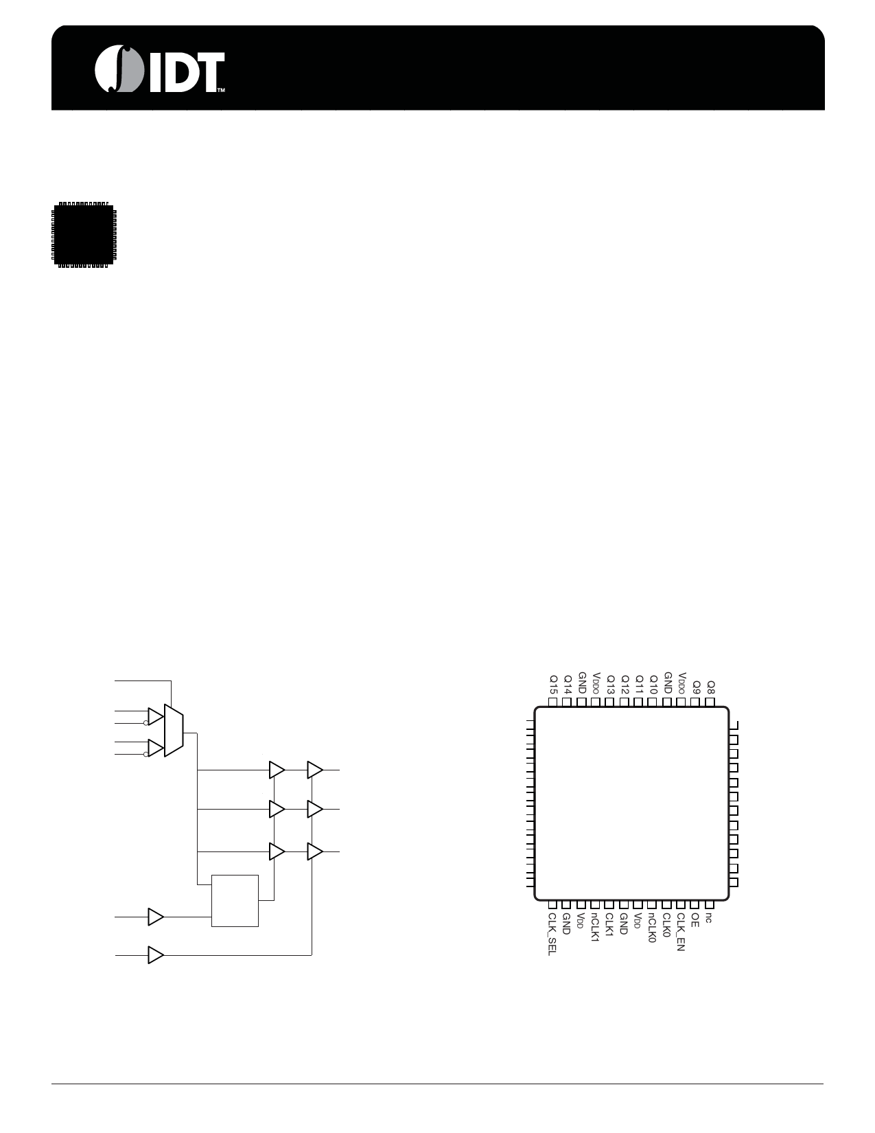
BLOCK DIAGRAM
PIN ASSIGNMENT
CLK_SEL
CLK0
nCLK0
0
CLK1
1
nCLK1
CLK_EN
LE
Q
nD
Q0:Q7
Q8:Q15
Q16:Q23
Q16
Q17
VDDO
GND
Q18
Q19
Q20
Q21
VDDO
GND
Q22
Q23
48 47 46 45 44 43 42 41 40 39 38 37
1
36
2
35
3
34
4
ICS8344-01 33
5
48-Lead LQFP
32
6 7mm x 7mm x 1.4mm 31
7
8
9
10
package body
Y Package
Top View
30
29
28
27
11
26
12
25
13 14 15 16 17 18 19 20 21 22 23 24
Q7
Q6
VDDO
GND
Q5
Q4
Q3
Q2
VDDO
GND
Q1
Q0
OE
The Preliminary Information presented herein represents a product in pre-production. The noted characteristics are based on initial product characterization
and/or qualification. Integrated Device Technology, Incorporated (IDT) reserves the right to change any circuitry or specifications without notice.
IDT™ / ICS™ LVCMOS/LVTTL FANOUT BUFFER
1
ICS8344AYI-01 REV. B MAY 10, 2007
Share Link: 