MAX1463 查看數據表(PDF) - Maxim Integrated
零件编号
产品描述 (功能)
生产厂家
MAX1463 Datasheet PDF : 50 Pages
| |||
Low-Power Two-Channel Sensor
Signal Processor
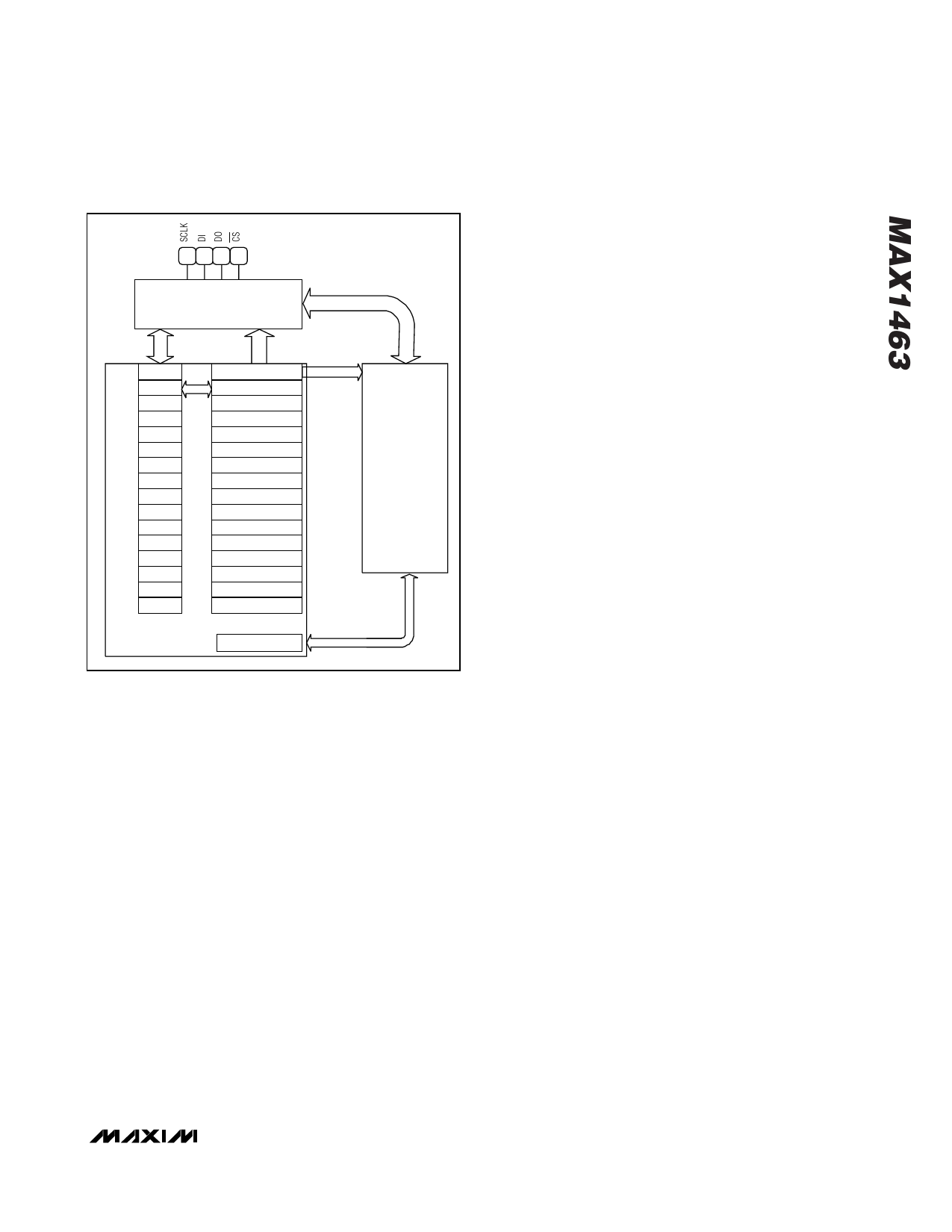
SERIAL INTERFACE
P0
P1
P2
CPU
P1
P3
P4
P5
P6
P7
P8
PA
PB
PC
PD
PE
PF
CPU PORTS
R0 POINTER (P)
R1 ACCUMULATOR (A)
R2
R3 MULTIPLICAND (N)
R4 MULTIPLIER (M)
R5 INDEX (I)
R6
R7
R8
R9
RA
RB
RC
RD
RE
RF
CPU REGISTERS
INSTRUCTION
ADDRESS
FLASH MEMORY
(4kB)
FLASH DATA
Figure 3. CPU Architecture
used to initiate a process (such as an ADC conversion or
a timer) or to turn modules on and off (such as op amps,
DAC outputs, PWM outputs, etc.) Table 3 lists the mod-
ule registers.
ADC Module
The ADC module (Figure 4) contains a 9-bit to 16-bit
sigma-delta converter with multiplexed differential and
single-ended signal inputs, a CO DAC, four reference
voltage inputs, two differential or four single-ended
external inputs, and 15 single-ended internal voltages
for measurement. The ADC output data is 16-bit two’s-
complement format. The conversion channel, modes,
and reference sources are all set in ADC configuration
registers. The conversion time is a function of the
selected resolution and ADC clock frequency. The CPU
can be programmed to convert any of the inputs and
the internal temperature sensor in any desired
sequence. For example, the differential inputs may be
converted many times and conversions of temperature
performed less frequently. See Table 4.
The ADC uses the internal 1.25V bandgap reference
(VBG) when converting the temperature input.
For any other conversions, the ADC reference can be
selected as VDD for conversions ratiometric to the
power supply, VREF pin for conversions relative to an
external voltage, and VBG x 4, which is an internally
generated “pseudo” 5.0V reference source. The ADC
voltage reference is also used by the CO DAC to main-
tain a signal conversion that is ratiometric to the select-
ed reference source.
The four analog inputs (INP1, INM1, INP2, INM2) and
several internal circuit nodes can be multiplexed to the
ADC for a single-ended conversion relative to VSS. The
selection of which circuit node is multiplexed to the ADC
is controlled by the ADC_Control register. The ADC can
measure each of the op-amp output nodes with gain for
converting user-defined circuits or incorporating system
diagnostic test functions. The DAC outputs can be con-
verted by the ADC with either op amp arranged as
unity-gain buffers on the DAC outputs. The internal
power nodes, VDD and VSS, and the bandgap reference
VBG can be multiplexed to the ADC for conversion as
well. These measurement modes are defined and initiat-
ed in the ADC_Control register. See Tables 5 and 7 for
the single-ended configuration.
ADC Registers
The ADC module has 10 registers for configuration,
control, and data output. There are three conversion
channels in the ADC; channel 1, channel 2, and tem-
perature. Channels 1 and 2 are associated with the dif-
ferential signal input pairs INP1-INM1 and INP2-INM2,
respectively. The temperature channel is associated
with the integrated temperature sensor. Each channel
has two configuration registers (ADC_Config_nA and
ADC_Config_nB where n = 1, 2, or T) for setting con-
version resolution, reference input, coarse offsets, etc.
The data output from a conversion of channel 1, 2, or T
is stored in the respective data output register
ADC_Data_n where n = 1, 2, or T. Each of the channels
can be used to convert single-ended inputs as listed in
Table 7. The ADC_Control register controls which chan-
nel is to be converted and what single-ended input, if
any, is to be directed to that channel. See Tables 8
through 13.
Conversion Start
To initiate an ADC conversion, a word is written to the
ADC_Control register with either CNVT1, CNVT2, or
CNVTT bit set to a 1 (Table 6). When an ADC conver-
sion is initiated, the CPU is halted and all CPU and
FLASH activities cease. All CNVT1, CNVT2, and CNVTT
bits are cleared after the ADC conversion is completed.
Upon completion of the conversion, the ADC result is
latched into the respective ADC_Data_n register. In
addition, the convert bits in control register 0 are all
______________________________________________________________________________________ 15
Share Link: 