MAX5059 查看數據表(PDF) - Maxim Integrated
零件编号
产品描述 (功能)
生产厂家
MAX5059 Datasheet PDF : 25 Pages
| |||
Parallelable Secondary-Side Synchronous Rectifier
Driver and Feedback-Generator Controller ICs
ABSOLUTE MAXIMUM RATINGS
V+ to GND .............................................................-0.3V to +30V
PGND to GND .......................................................-0.3V to +0.3V
COMPV, VREG, VDR, TSF to GND......................... -0.3V to +14V
All Other Pins to GND ..................................-0.3V to (VP + 0.3V)
VREG Source Current .........................................................50mA
COMPV, RMGU, RMGD, TSF Sink Current ....................... 30mA
VP to GND ................................................................-0.3V to +6V
VSO, CSO Source/Sink Current ......................................... ±5mA
SFP Source Current ............................................................. 5mA
QREC, QSYNC Continuous Current....................................50mA
QREC, QSYNC Current < 500ns..............................................5A
Continuous Power Dissipation (TA = +70°C)
28-Pin TSSOP (derate 23.8mW/°C above +70°C). ....1905mW
Junction Temperature ......................................................+150°C
Operating Temperature Ranges
MAX5058EUI, MAX5059EUI ............................-40°C to +85°C
MAX5058AUI, MAX5059AUI..........................-40°C to +125°C
Storage Temperature Range .............................-65°C to +150°C
Lead Temperature (soldering, 10s) .................................+300°C
Stresses beyond those listed under “Absolute Maximum Ratings” may cause permanent damage to the device. These are stress ratings only, and functional
operation of the device at these or any other conditions beyond those indicated in the operational sections of the specifications is not implied. Exposure to
absolute maximum rating conditions for extended periods may affect device reliability.
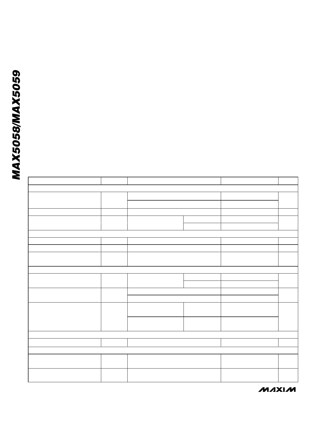
ELECTRICAL CHARACTERISTICS
(V+ = +12V, GND = PGND = 0, VDR = VREG, CQSYNC = CQREC = 0, ZCP = ZCN = BUFIN = CSP = CSN = SFN = VSN = GND, VIREF =
VVSP = 1.785V, CVREG = 2.2µF, CVP = 1µF, CCOMPS = 0.1µF, CSFP = 68nF, TA = TMIN to TMAX, unless otherwise noted. Typical values
are at TA = +25°C.)
PARAMETER
POWER SUPPLY
SYMBOL
Supply Voltage Range
V+
Quiescent Supply Current
IQ
Switching Supply Current
ISW
IREF: REFERENCE CURRENT OUTPUT
Reference Current
IIREF
Reference Current Variation
ΔIIREF
Reference Voltage Compliance
Range
VREG: LOW-DROPOUT REGULATOR
Regulator Output
VVREG
Line Regulation
Dropout
VDROP
VP: INTERNAL REGULATOR
Regulator Output Setpoint
VVP
ZC: ZERO-CURRENT COMPARATOR
CONDITIONS
MAX5058
MAX5059
fSW = 250kHz at BUFIN
MAX5058
MAX5059
VIREF = 1.785V
VIREF = 0.5V to 2.5V
Guaranteed by reference current variation
test
IVREG = 0 to 30mA
MAX5058
MAX5059
MAX5058, V+ = 6V to 28V
MAX5059, V+ = 11V to 28V
MAX5058
V+ = 4.5V,
IVREG = 30mA
MAX5059
V+ = 9.3V,
IVREG = 30mA
IVP = 0 to 5mA
MIN TYP MAX UNITS
4.5
28.0
V
9.3
28.0
2.5
5
mA
4.5
mA
6
49.2
50
51.1
µA
-0.1
+0.1 %/V
0.5
2.5
V
4.75
5
5.25
V
9.4
10
10.6
25
mV
25
200 350
mV
200 350
3.8
4.3
V
Zero-Current Comparator
Threshold
VZCTH TA = +25°C
+3.5
+5
+6.5
mV
Zero-Current Comparator Input
Current
IZC
-2.5
+2.5
µA
2 _______________________________________________________________________________________
Share Link: 