AM29LV160BT-80FC 查看數據表(PDF) - Advanced Micro Devices
零件编号
产品描述 (功能)
生产厂家
AM29LV160BT-80FC
Advanced Micro Devices
AM29LV160BT-80FC Datasheet PDF : 46 Pages
| |||
PRELIMINARY
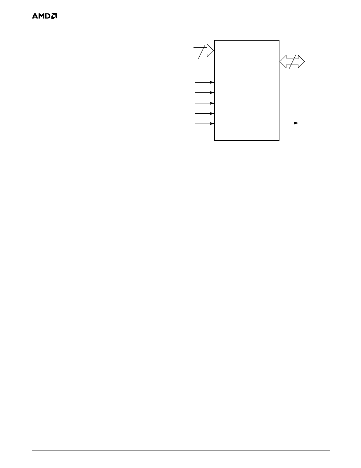
PIN CONFIGURATION
A0–A19 =
DQ0–DQ14 =
DQ15/A-1 =
BYTE# =
CE#
=
OE#
=
WE#
=
RESET# =
RY/BY# =
VCC
=
20 addresses
15 data inputs/outputs
DQ15 (data input/output, word mode),
A-1 (LSB address input, byte mode)
Selects 8-bit or 16-bit mode
Chip enable
Output enable
Write enable
Hardware reset pin
Ready/Busy output
(N/A SO 044)
3.0 volt-only single power supply
(see Product Selector Guide for speed
options and voltage supply tolerances)
VSS
= Device ground
NC
= Pin not connected internally
LOGIC SYMBOL
20
A0–A19
16 or 8
DQ0–DQ15
(A-1)
CE#
OE#
WE#
RESET#
BYTE#
RY/BY#
(N/A SO 044)
21358F-4
6
Am29LV160B
Share Link: 