NT7701 查看數據表(PDF) - Novatek Microelectronics
零件编号
产品描述 (功能)
生产厂家
NT7701 Datasheet PDF : 37 Pages
| |||
NT7701
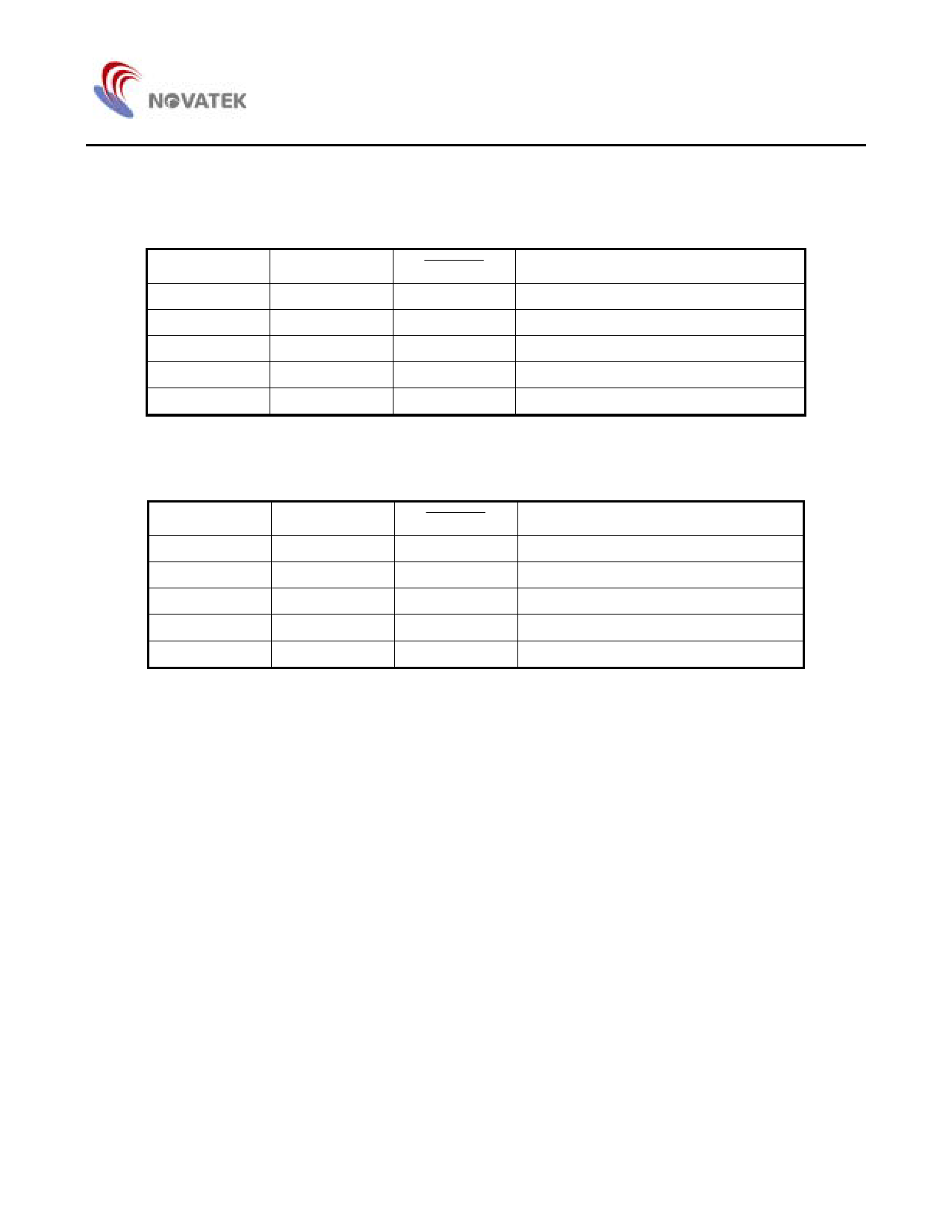
2. LCD Driver Output Voltage Level
The relationship amongst the data bus signal, AC converted signal FR and LCD driver output voltage is as shown in the table
below:
2.1. Segment Mode
FR
Latch Data
DISPOFF
Driver Output Voltage Level (Y1 - Y160)
L
L
H
V43
L
H
H
V5
H
L
H
V12
H
H
H
V0
X
X
L
V5
Here, VSS ≤ V5 < V43 < V12 <V0, H: VDD (+2.5 to +5.5V), L: VSS (0V), X: Don't care
2.2. Common Mode
FR
L
L
H
H
X
Latch Data
L
H
L
H
X
DISPOFF
H
H
H
H
L
Driver Output Voltage Level (Y1 - Y160)
V43
V0
V12
V5
V5
Here, VSS ≤ V5 < V43 < V12 < V0, H: VDD (+2.5 to +5.5V), L: VSS (0V), X: Don't care
Note: There are two kinds of power supply (logic level voltage, LCD driver voltage) for the LCD driver. Please supply regular
voltage, which assigned by specification for each power pin.
That time "Don't care" should be fixed to "H" or "L", avoiding floating.
11
Share Link: 