IDT71215S8 查看數據表(PDF) - Integrated Device Technology
零件编号
产品描述 (功能)
生产厂家
IDT71215S8
Integrated Device Technology
IDT71215S8 Datasheet PDF : 14 Pages
| |||
IDT71215
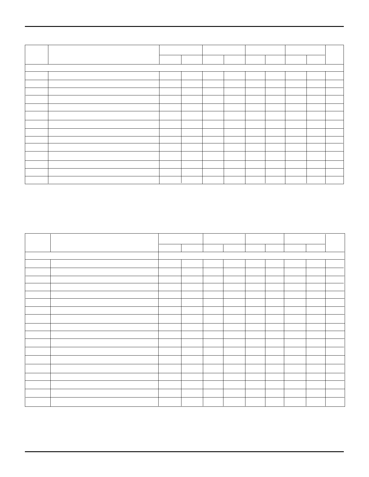
BiCMOS 16Kx15 CACHE-TAG RAM
AC ELECTRICAL CHARACTERISTICS
(VCC = 5.0V ± 5%, VCCQ = 5.0V ± 5% OR 3.3V ± 0.3V, TA = 0 to 70°C)
COMMERCIAL TEMPERATURE RANGE
IDT71215S8
IDT71215S9 IDT71215S10
Symbol Parameter
Min. Max. Min. Max. Min. Max.
Read Cycle
tAAT
Address Access Time Tag Bits
—
10
—
11
—
12
tACST Chip Select Access Time Tag Bits
—
8
—
9
—
10
tCLZ(1) Chip Select to Tag and Status Bits in Low-Z 1
—
1
—
1
—
tCHZ(1) Chip Select to Tag and Status Bits in High-Z 1
5
1
6
1
6
tOET Output Enable to Tag Bits Valid
—
5
—
6
—
6
tOTLZ(1) Output Enable to Tag Bits in Low-Z
0
—
0
—
0
—
tOTHZ(1)
tTOH
tOES
tOSLZ(1)
tOSHZ(1)
tAAS
Output Enable to Tag Bits in High-Z
Tag Bit Hold from Address Change
Output Enable to Status Bits Valid
Output Enable to Status Bits in Low-Z
Output Enable to Status Bits in High-Z
Address Access Time Status Bits
1
5
1
6
1
6
2
—
2
—
2
—
—
5
—
6
—
6
0
—
0
—
0
—
1
5
1
6
1
6
—
8
—
9
—
10
tACSS Chip Select Access Time Status Bits
—
6
—
7
—
8
tSOH Status Bit Hold from Address Change
2
—
2
—
2
—
NOTE:
1. This parameter is guaranteed with the AC Load (Figure 3) by device characterization, but is not production tested.
IDT71215S12
Min. Max. Unit
— 14
ns
— 12
ns
1—
ns
1
7
ns
—7
ns
0—
ns
1
7
ns
2—
ns
—7
ns
0—
ns
1
7
ns
— 12
ns
— 10
ns
2—
ns
3075 tbl 11
AC ELECTRICAL CHARACTERISTICS (1)
(VCC = 5.0V ± 5%, VCCQ = 5.0V ± 5% OR 3.3V ± 0.3V, TA = 0 to 70°C)
IDT71215S8 IDT71215S9 IDT71215S10
Symbol
Parameter
Reset and Power Down Cycles
Min. Max. Min. Max. Min. Max.
tSR
RESET Set-up Time
4
—
4
—
4
—
tHR
tSRST
RESET Hold Time
Status Bit Reset Time
1
—
1
—
1
—
—
50
—
60
—
60
tSHRS Status Bit Hold from RESET LOW
2
—
2
—
2
—
tRSMI RESET LOW to MATCH and BRDY Invalid
—
9
—
10
—
10
tRSMV RESET HIGH to MATCH and BRDY Valid
—
110 —
120
—
120
tRSHZ(2) RESET LOW to TAG High-Z
—
9
—
10
—
10
tRSLZ(2) RESET HIGH to TAG Low-Z
—
90
—
100
—
100
tPDSR
tRHPL
tRHWL
tPD(2)
tPU(2)
PWRDN Set-up to RESET LOW
RESET HIGH to PWDRN LOW
RESET HIGH to WET and WES LOW
PWRDN LOW to Low Power Mode
PWRDN HIGH to Active Power Mode
30
—
30
—
30
—
1
—
1
—
1
—
90
—
95
—
95
—
—
50
—
50
—
50
0
—
0
—
0
—
tPDHZ(2) PWRDN LOW to Outputs in High-Z
—
9
—
10
—
10
tPDLZ(2) PWRDN HIGH to Outputs in Low-Z
0
—
0
—
0
—
tPUV
PWRDN HIGH to Outputs Valid
tWHPL(2) WET and WES HIGH to PWRDN LOW
—
50
—
50
—
50
5
—
5
—
5
—
tPUWL PWRDN HIGH to WET and WES Active
50
—
50
—
50
—
NOTES:
1. Power-down mode is intended to be used during extended time periods of device inactivity.
2. This parameter is guaranteed with the AC Load (Figure 3) by device characterization, but is not production tested.
IDT71215S12
Min. Max. Unit
4
—
ns
1
—
ns
—
70
ns
2
—
ns
—
12
ns
—
130 ns
—
12
ns
—
110 ns
30
—
ns
1
— CLK
105
—
ns
—
50
ns
0
—
ns
—
12
ns
0
—
ns
—
50
ns
5
—
ns
50
—
ns
3075 tbl 12
14.3
7
Share Link: 