GD25Q20BSIGY 查看數據表(PDF) - Unspecified
零件编号
产品描述 (功能)
生产厂家
GD25Q20BSIGY Datasheet PDF : 38 Pages
| |||
GD2U5nQif2or0mBSxeIcGtoxr Uniform sector dual and quad serial flash
Dual and Quad Serial Flash
GD25Q40B/20B
8. ELECTRICAL CHARACTERISTICS
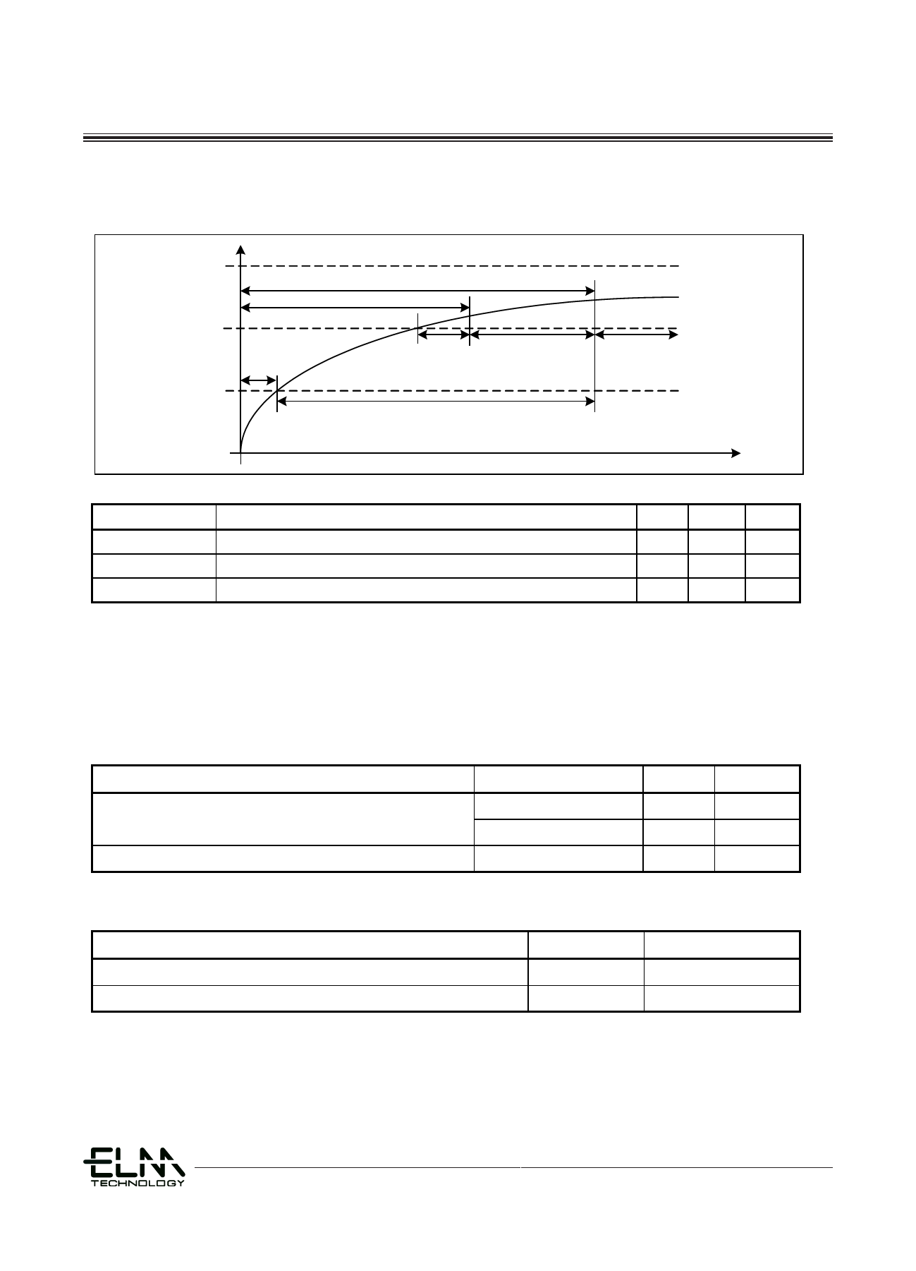
8.1. POWER-ON TIMING
Vcc(max)
Program, Erase and Write command are ignored
Chip Selection is not allowed
Vcc(min)
Reset
State
VWI
tVSL
Read command
is allowed
tPUW
Device is fully
accessible
Time
Symbol
tVSL
tPUW
VWI
Table3. Power-Up Timing and Write Inhibit Threshold
Parameter
VCC(min) to CS# Low
Time Delay Before Write Instruction
Write Inhibit Voltage
Min
10
1
1
Max
10
2.5
Unit
us
ms
V
8.2. INITIAL DELIVERY STATE
The device is delivered with the memory array erased: all bits are set to 1(each byte contains FFH).The Status Register
contains 00H (all Status Register bits are 0).
8.3. DATA RETENTION AND ENDURANCE
Parameter
Minimum Pattern Data Retention Time
Erase/Program Endurance
Test Condition
150�
125�
-40 to 85�
Min
10
20
100K
Units
Years
Years
Cycles
8.4. LATCH UP CHARACTERISTICS
Parameter
Input Voltage Respect To VSS On I/O Pins
VCC Current
Min
-1.0V
-100mA
Max
VCC+1.0V
100mA
34
38 - 29
Rev.1.1
Share Link: 