EVAL-ADF4151EB1Z 查看數據表(PDF) - Analog Devices
零件编号
产品描述 (功能)
生产厂家
EVAL-ADF4151EB1Z Datasheet PDF : 28 Pages
| |||
ADF4151
FAST LOCK—AN EXAMPLE
If a PLL has a reference frequency of 13 MHz, a fPFD of 13 MHz
and a required lock time of 50 µs, the PLL is set to wide bandwidth
for 40 µs. This example assumes a modulus of 65 for channel
spacing of 200 kHz.
If the time period set for the wide bandwidth is 40 µs, then
Fast Lock Timer Value = Time In Wide Bandwidth × fPFD/MOD
Fast Lock Timer Value = 40 µs × 13 MHz/65 = 8
Therefore, 8 must be loaded into the clock divider value in
Register 3 in Step 1 of the sequence described in the Fast Lock
Timer and Register Sequences section.
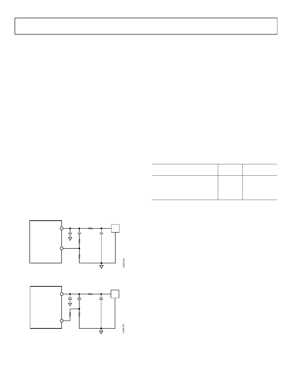
FAST LOCK—LOOP FILTER TOPOLOGY
To use fast lock mode, the damping resistor in the loop filter
is reduced to ¼ of its value while in wide bandwidth mode. To
achieve the wider loop filter bandwidth, the charge pump
current increases by a factor of 16. To maintain loop stability,
the damping resistor must be reduced a factor of ¼. To enable
fast lock, the SW pin is shorted to the GND pin by setting
Bits[DB16:DB15] in Register 3 to values 0, 1. The following two
topologies are available:
• The damping resistor (R1) is divided into two values (R1
and R1A) that have a ratio of 1:3 (see Figure 26).
• An extra resistor (R1A) is connected directly from SW,
as shown in Figure 27. The extra resistor is calculated
such that the parallel combination of an extra resistor
and the damping resistor (R1) is reduced to ¼ of the
original value of R1 (see Figure 27).
ADF4151
CPOUT
C1
SW
R2
C2
R1
VCO
C3
R1A
Figure 26. Fast Lock Loop Filter Topology—Topology 1
ADF4151
CPOUT
C1
R2
C2
VCO
C3
R1A
R1
SW
Figure 27. Fast Lock Loop Filter Topology—Topology 2
Data Sheet
SPUR MECHANISMS
This section describes the three different spur mechanisms that
arise with a fractional-N synthesizer and how to minimize them
in the ADF4151.
Fractional Spurs
The fractional interpolator in the ADF4151 is a third-order Σ-Δ
modulator (SDM) with a modulus (MOD) that is programmable
to any integer value from 2 to 4095. In low spur mode (dither
enabled), the minimum allowable value of MOD is 50. The
SDM is clocked at the PFD reference rate (fPFD) that allows PLL
output frequencies to be synthesized at a channel step resolution
of fPFD/MOD.
In low noise mode (dither off), the quantization noise from the
Σ-Δ modulator appears as fractional spurs. The interval between
spurs is fPFD/L, where L is the repeat length of the code sequence
in the digital Σ-Δ modulator. For the third-order modulator
used in the ADF4151, the repeat length depends on the value
of MOD, as listed in Table 7.
Table 7. Fractional Spurs with Dither Off
Condition (Dither Off)
Repeat
Length
If MOD is divisible by 2, but not 3 2 × MOD
If MOD is divisible by 3, but not 2 3 × MOD
If MOD is divisible by 6
6 × MOD
Otherwise
MOD
Spur Interval
Channel step/2
Channel step/3
Channel step/6
Channel step
In low spur mode (dither on), the repeat length is extended to
221 cycles, regardless of the value of MOD, which makes the
quantization error spectrum look like broadband noise. This
may degrade the in-band phase noise at the PLL output by as
much as 10 dB. For lowest noise, dither off is a better choice,
particularly when the final loop bandwidth is low enough to
attenuate even the lowest frequency fractional spur.
Integer Boundary Spurs
Another mechanism for fractional spur creation is the interactions
between the RF VCO frequency and the reference frequency.
When these frequencies are not integer related (the point of a
fractional-N synthesizer) spur sidebands appear on the VCO
output spectrum at an offset frequency that corresponds to the
beat note or difference frequency between an integer multiple of
the reference and the VCO frequency. These spurs are attenuated
by the loop filter and are more noticeable on channels close to
integer multiples of the reference where the difference frequency
can be inside the loop bandwidth; therefore, the name integer
boundary spurs.
Rev. B | Page 22 of 28
Share Link: 