ADG726 وں¥çœ‹و•¸و“ڑè،¨ï¼ˆPDF) - Analog Devices
零ن»¶ç¼–هڈ·
ن؛§ه“پوڈڈè؟° (هٹں能)
ç”ںن؛§هژ‚ه®¶
ADG726 Datasheet PDF : 12 Pages
| |||
TIMING CHARACTERISTICS1, 2, 3
Parameter
Limit at TMIN, TMAX
Unit
t1
0
t2
0
t3
10
t4
10
t5
5
t6
2
ns min
ns min
ns min
ns min
ns min
ns min
NOTES
1See Figure 1.
2All input signals are specified with tr = tf = 1 ns (10% to 90% of VDD).
3Guaranteed by design and characterization, not production tested.
Specifications subject to change without notice.
ADG726/ADG732
Conditions/Comments
CS to WR Setup Time
CS to WR Hold Time
WR Pulsewidth
Time between WR Cycles
Address, Enable Setup Time
Address, Enable Hold Time
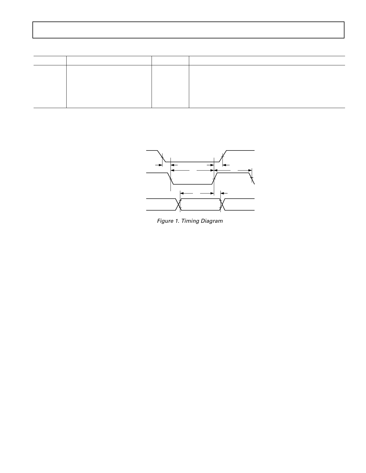
CS
t1
t2
t3
t4
WR
A0, A1, A2, A3, (A4)
EN
t5
t6
Figure 1. Timing Diagram
Figure 1 shows the timing sequence for latching the switch
address and enable inputs. The latches are level sensitive; there-
fore, while WR is held low, the latches are transparent and the
switches respond to changing the address and enable the inputs.
Input data is latched on the rising edge of WR. The ADG726
has two CS inputs. This enables the part to be used either as a
dual 16-1 channel multiplexer or a differential 16-channel
multiplexer. If a differential output is required, tie CSA and
CSB together.
REV. 0
–5–
Share Link: 