ADG812(RevD) 查看數據表(PDF) - Analog Devices
零件编号
产品描述 (功能)
生产厂家
ADG812 Datasheet PDF : 15 Pages
| |||
Data Sheet
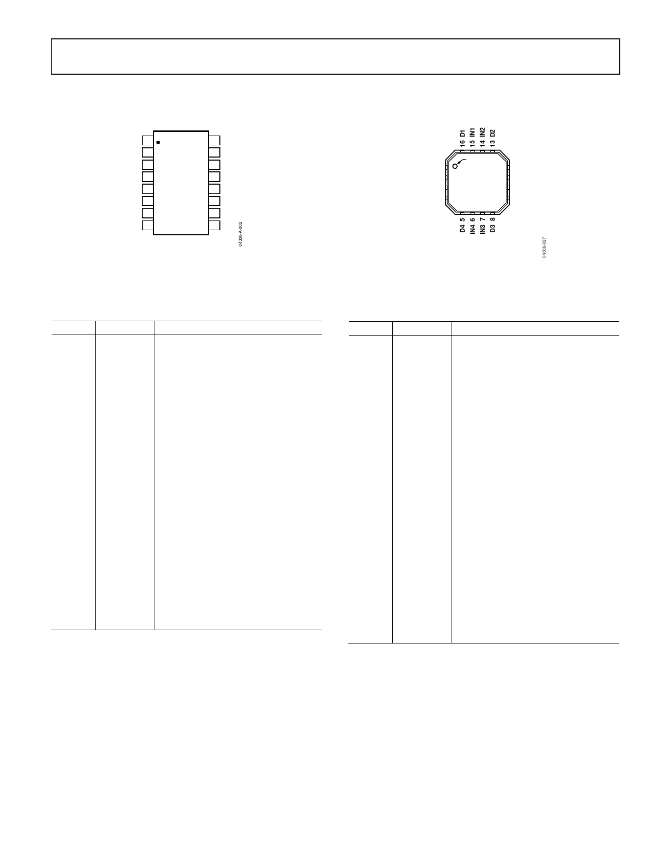
PIN CONFIGURATIONS AND FUNCTION DESCRIPTIONS
ADG811/ADG812
IN1 1
D1 2
S1 3
NIC 4
GND 5
S4 6
D4 7
IN4 8
16 IN2
15 D2
ADG811/
ADG812
TOP VIEW
(Not to Scale)
14 S2
13 VDD
12 NIC
11 S3
10 D3
9 IN3
NIC = NO INTERNAL CONNECTION
Figure 3. ADG811/ADG812 Pin Configuration (16-Lead TSSOP)
Table 6. ADG811/ADG812 Pin Function Descriptions (16-Lead TSSOP)
Pin No.
TSSOP
LFCSP
Mnemonic
Description
1
15
IN1
Logic control input.
2
16
D1
Drain Terminal. This pin may be an input or output.
3
1
S1
Source Terminal. This pin may be an input or output.
4, 12
2, 10
NIC
No Internal Connection.
5
3
GND
Ground (0 V) reference.
6
4
S4
Source Terminal. This pin may be an input or output.
7
5
D4
Drain Terminal. This pin may be an input or output.
8
6
IN4
Logic Control Input.
9
7
IN3
Logic Control Input.
10
8
D3
Drain Terminal. This pin may be an input or output.
11
9
S3
Source Terminal. This pin may be an input or output.
13
11
VDD
Most Positive Power Supply Potential.
14
12
S2
Source Terminal. This pin may be an input or output.
15
13
D2
Drain Terminal. This pin may be an input or output.
16
14
IN2
Logic Control Input.
Not applicable
17
EPAD
Exposed Pad. Connect exposed pad to GND.
Rev. D | Page 7 of 15
Share Link: 