AMMC004AWP 查看數據表(PDF) - Advanced Micro Devices
零件编号
产品描述 (功能)
生产厂家
AMMC004AWP Datasheet PDF : 39 Pages
| |||
PRELIMINARY
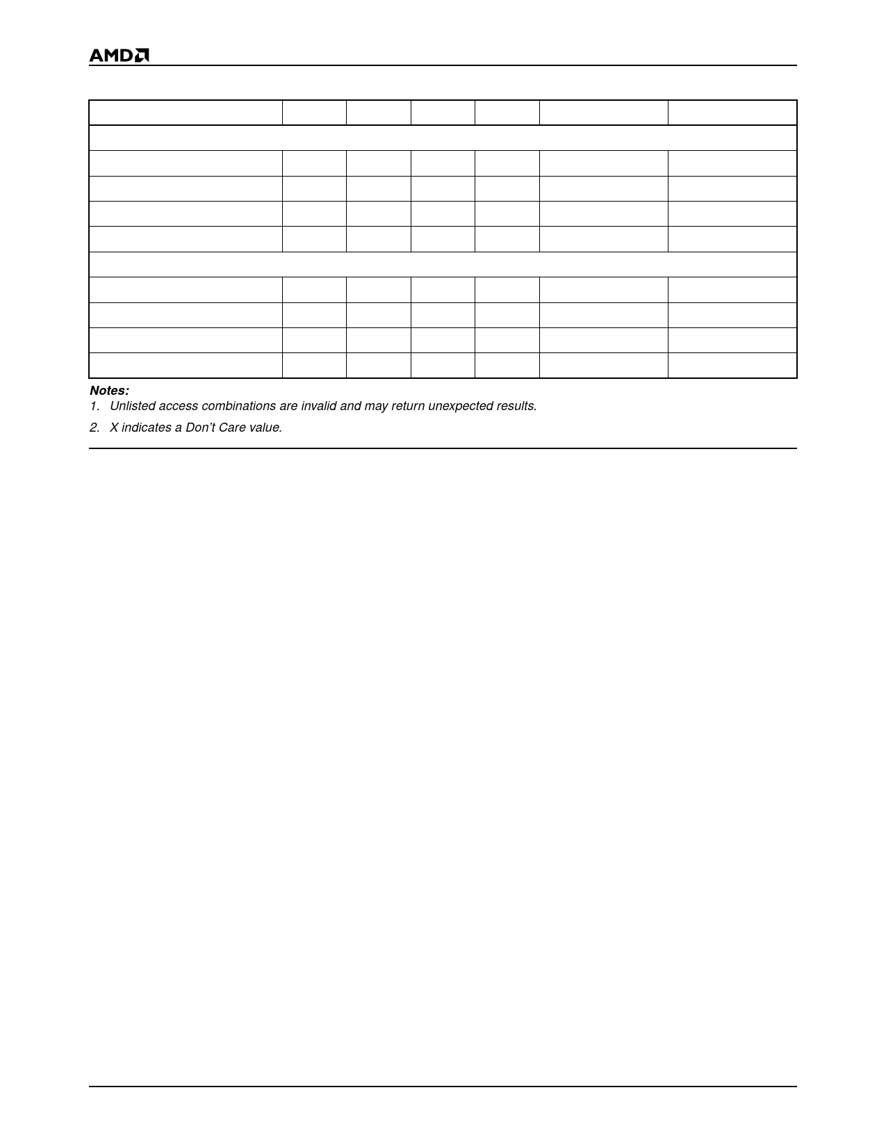
Table 4. Miniature Card Read/Write Modes
Function
CEH# CEL#
WE#
OE#
Read Mode
Standby
H
H
X
X
Word Access
L
L
H
L
Low Byte Access
H
L
H
L
High Byte Access
L
H
H
L
Write Mode
Standby
H
H
X
X
Word Access
L
L
L
H
Low Byte Access
H
L
L
H
High Byte Access
L
H
L
H
Notes:
1. Unlisted access combinations are invalid and may return unexpected results.
2. X indicates a Don’t Care value.
D8–D15
High-Z
High Byte Data
High-Z
High Byte Data
High-Z
High Byte Data
High-Z
High Byte Data
D0–D7
High-Z
Low Byte Data
Low Byte Data
High-Z
High-Z
Low Byte Data
Low Byte Data
High-Z
Erase Operations
The AMD Flash Miniature Card is organized as an array
of individual devices. On the 2 Mbyte Miniature Card,
each Am29F080B device contains sixteen 64 Kbyte sec-
tors, for a total of 1 Mbyte of memory space per device.
On 4 and 8 Mbyte Miniature Cards, each Am29F017B
device contains thirty-two 64 Kbyte sectors, for a total of
2 Mbytes of memory space per device.
Flash technology allows any logical “1” data bit to be pro-
grammed to a logical “0”. The only way to reset bits to a
logical “1” is to erase that entire memory sector or
memory device. Once a memory sector or memory
device is erased, any address location may be pro-
grammed. Two or more devices may be erased concur-
rently when additional ICC current is supplied to the card.
However, erasing more than two devices concurrently is
not typical in battery-powered applications, but may take
place during procedures such as card testing.
Since erase commands operate on entire sectors or
devices, the host should track the affected memory
addresses; for example, by determining the sector size
and device size and calculating the corresponding
addresses.
Erase operations can be performed in several ways:
s Erase a single sector or multiple sectors in a device
s Erase a sector pair
s Erase multiple device pairs *
s Erase the entire card *
* This operation is only feasible in solutions capable of
supplying more than the specified miniature card
supply current requirement (150 mA) per system. Each
AMD Flash memory device pair will require a
maximum of 120 mA supply current.
The common memory space data contents are altered
in a similar manner as writing to individual Flash memory
devices. An on-card address decoder activates the
appropriate Flash device in the memory array. Each
device internally latches address and data during write
cycles. Refer to Table 4.
Word-Wide Operations
The AMD Miniature Card provide the flexibility to operate
on data in a byte-wide or word-wide format. In word-wide
operations, the low bytes are controlled with CEL#. The
high bytes are controlled with CEH#. Refer to the block
diagram for more information.
Byte-Wide Operations
Byte-wide data is available for read and write opera-
tions (CEL# = 0, CEH# = 1). Even and odd bytes are
stored in separate memory devices (for example, S0
and S1) and are accessed by controlling CEL# and
CEH#. The even byte is the low order byte and the odd
byte is the high order byte of a 16-bit word.
Each memory sector or device pair must be addressed
separately for erase operations. Refer to the block
diagram for more information.
Card Detection
Each CD# (output) pin should be detected by the host
system to determine if the memory card is adequately
seated in the socket. CD# and CINS# are internally tied
to ground. If both bits are not detected, the system
should indicate that the card must be re-inserted.
10
AmMC0XXA
Share Link: 