BA00BC0W 查看數據表(PDF) - ROHM Semiconductor
零件编号
产品描述 (功能)
生产厂家
BA00BC0W Datasheet PDF : 19 Pages
| |||
BAxxBC0 Series BAxxBC0W Series BA00BC0WCP-V5
Datasheet
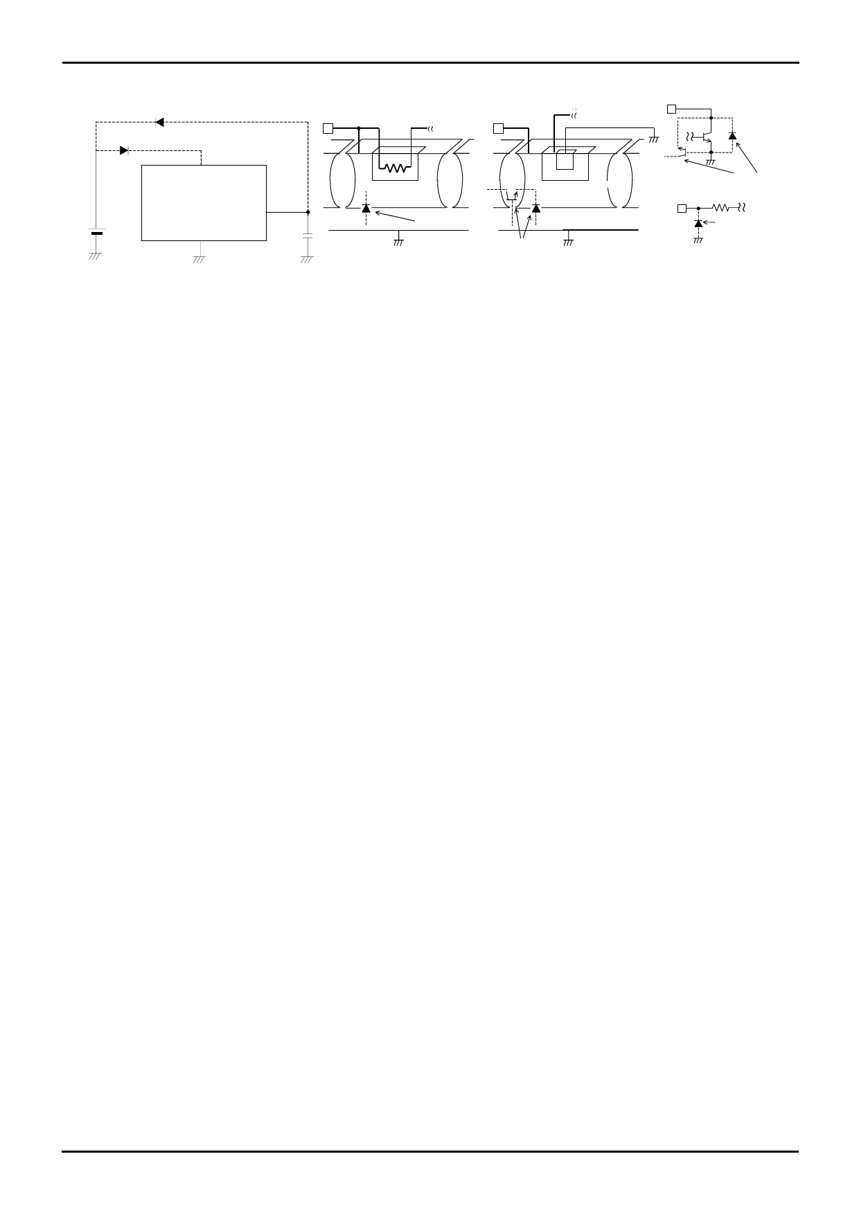
Bypass Diode
Diode for preventing back current flow
VCC
Output pin
Fig.23 Bypass Diode
((P端IN子AA))
P+
N
PPs基ub板strate
R抵es抗istor
Trトanラsンistジorス(NタP(NNP) N)
((端P子INBB)) C
B
E
(PINB)
P
N
P+
N
Pa寄ra生sit素ic 子elements
P+
N
GND
Parasitic elements
N
PP
NN
GND
P+
N
N
(PINA)
P subPst基ra板te
GND
C
B
E
GND
Parasitic elements or
transistors
Parasitic elements
GND
Fig.24 Example of Simple Bipolar IC Architecture
Status of this document
The Japanese version of this document is formal specification. A customer may use this translation version only for a reference
to help reading the formal version.
If there are any differences in translation version of this document formal version takes priority.
www.rohm.com
© 2012 ROHM Co., Ltd. All rights reserved.
TSZ22111・15・001
11/16
TSZ02201-0R6R0A600120-1-2
26.Jun.2012 Rev.001
Share Link: 