BD8966FVM-TR(2009) 查看數據表(PDF) - ROHM Semiconductor
零件编号
产品描述 (功能)
生产厂家
BD8966FVM-TR
(Rev.:2009)
(Rev.:2009)
ROHM Semiconductor
BD8966FVM-TR Datasheet PDF : 15 Pages
| |||
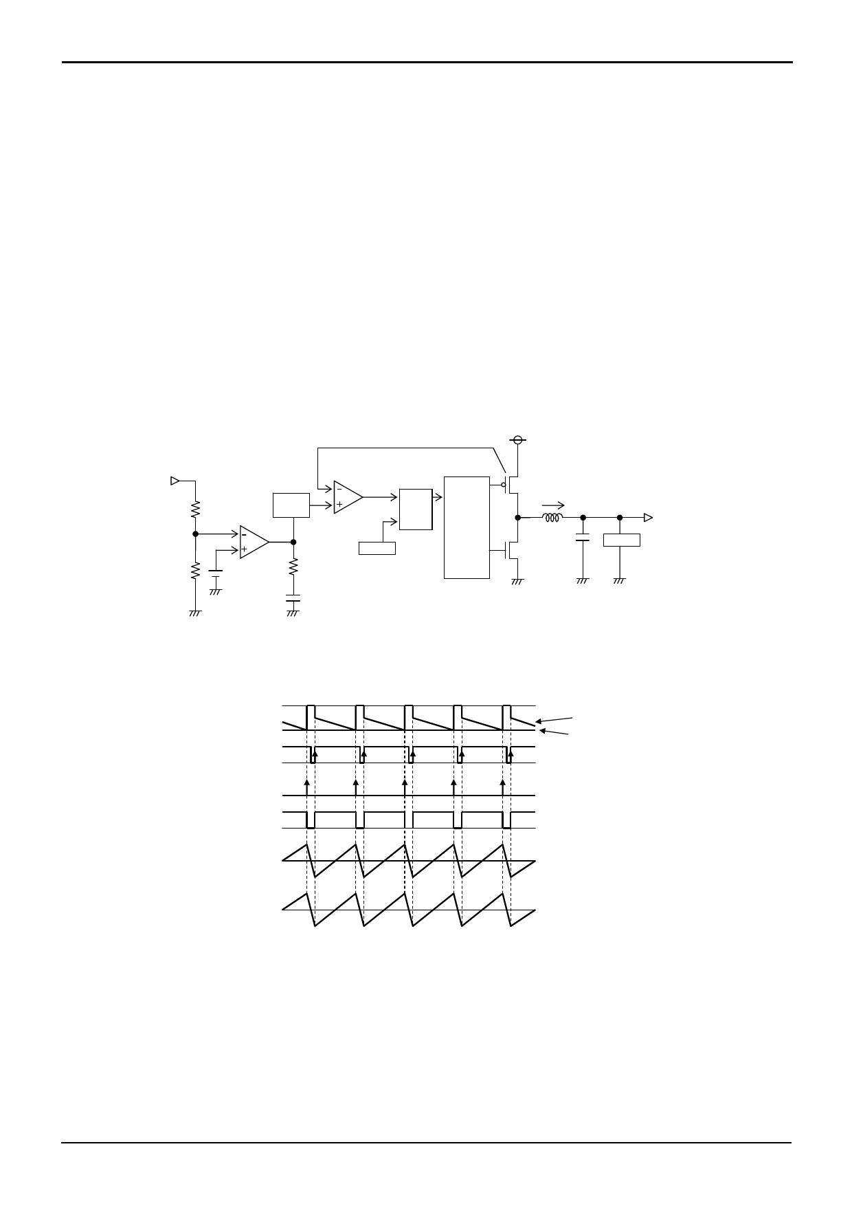
BD8966FVM
Technical Note
●Switching regulator efficiency
Efficiency ŋ may be expressed by the equation shown below:
η= VOUT×IOUT ×100[%]= POUT ×100[%]=
Vin×Iin
Pin
POUT
×100[%]
POUT+PDα
Efficiency may be improved by reducing the switching regulator power dissipation factors PDα as follows:
Dissipation factors:
1) ON resistance dissipation of inductor and FET:PD(I2R)
2) Gate charge/discharge dissipation:PD(Gate)
3) Switching dissipation:PD(SW)
4) ESR dissipation of capacitor:PD(ESR)
5) Operating current dissipation of IC:PD(IC)
1)PD(I2R)=IOUT2×(RCOIL+RON) (RCOIL[Ω]:DC resistance of inductor, RON[Ω]:ON resistance of FET, IOUT[A]:Output
current.)
2)PD(Gate)=Cgs×f×V (Cgs[F]:Gate capacitance of FET, f[Hz]:Switching frequency, V[V]:Gate driving voltage of FET)
Vin2×CRSS×IOUT×f
3)PD(SW)=
IDRIVE
(CRSS[F]:Reverse transfer capacitance of FET, IDRIVE[A]:Peak current of gate.)
4)PD(ESR)=IRMS2×ESR (IRMS[A]:Ripple current of capacitor、ESR[Ω]:Equivalent series resistance.)
5)PD(IC)=Vin×ICC (ICC[A]:Circuit current.)
www.rohm.com
© 2009 ROHM Co., Ltd. All rights reserved.
8/14
2009.05 - Rev.A
Share Link: 