BYS10-45HE3/TR 查看數據表(PDF) - Vishay Semiconductors
零件编号
产品描述 (功能)
生产厂家
BYS10-45HE3/TR Datasheet PDF : 4 Pages
| |||
www.vishay.com
BYS10-25 thru BYS10-45
Vishay General Semiconductor
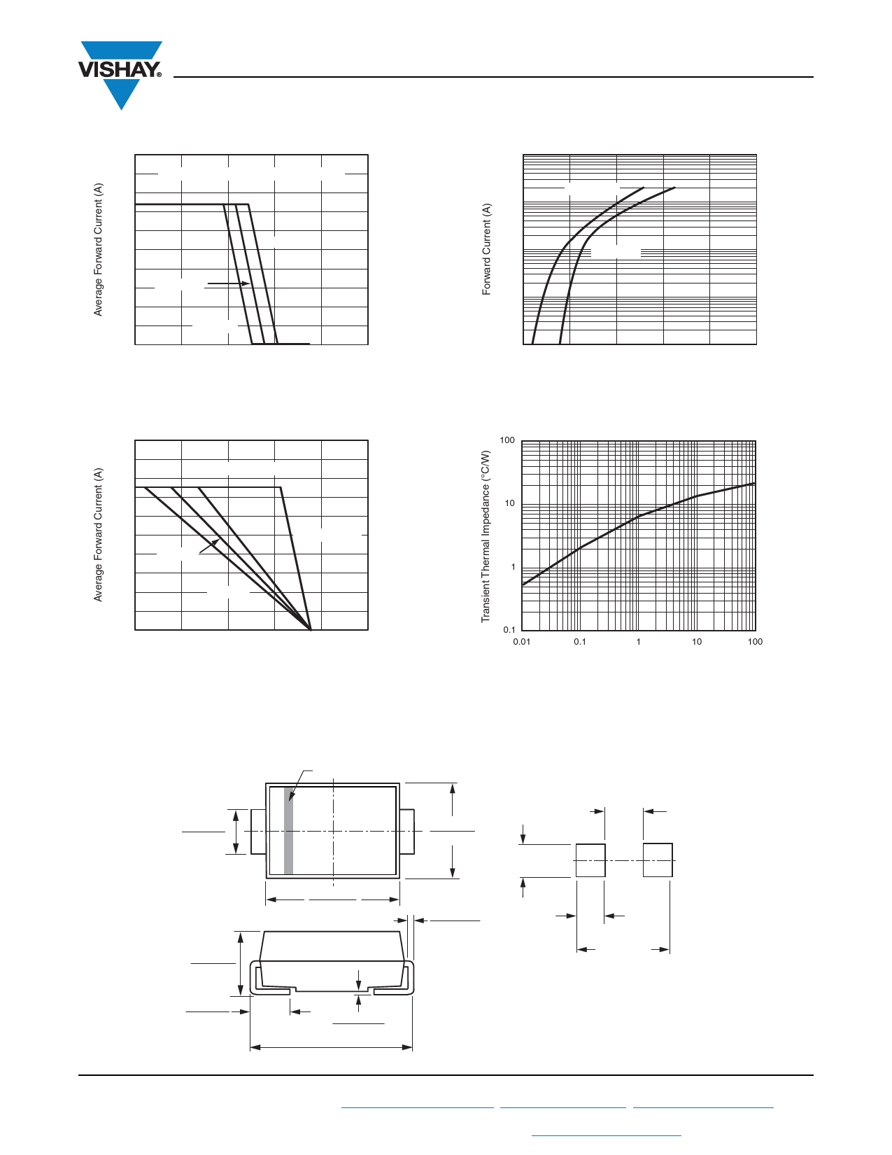
2.0
VR = VRRM, Half Sine-Wave, RthJA = 25 K/W
1.6
1.2
BYS10-25
0.8
BYS10-35
0.4
0
0
BYS10-45
40
80
120
160
200
Ambient Temperature (°C)
Fig. 3 - Max. Average Forward Current vs. Ambient Temperature
100
TJ = 150 °C
10
1
TJ = 25 °C
0.1
0.01
0
0.4
0.8
1.2
1.6
2.0
Forward Voltage (V)
Fig. 5 - Max. Forward Current vs. Forward Voltage
2.0
100
VR = 0 V, Half Sine-Wave
1.6
10
1.2
100 K/W
RthJA = 25 K/W
0.8
125 K/W
1
0.4
150 K/W
0
0
40
80
120
160
200
Ambient Temperature (°C)
Fig. 4 - Max. Average Forward Current vs. Ambient Temperature
0.1
0.01
0.1
1
10
100
t - Heating Time (s)
Fig. 6 - Typical Transient Thermal Impedance
PACKAGE OUTLINE DIMENSIONS in inches (millimeters)
DO-214AC (SMA)
Cathode Band
0.065 (1.65)
0.049 (1.25)
0.110 (2.79)
0.100 (2.54)
Mounting Pad Layout
0.066 (1.68)
MIN.
0.074 (1.88)
MAX.
0.090 (2.29)
0.078 (1.98)
0.177 (4.50)
0.157 (3.99)
0.012 (0.305)
0.006 (0.152)
0.060 (1.52)
MIN.
0.208 (5.28)
REF.
0.060 (1.52)
0.030 (0.76)
0.008 (0.203)
0 (0)
0.208 (5.28)
0.194 (4.93)
Revision: 26-Mar-12
3
Document Number: 86013
For technical questions within your region: DiodesAmericas@vishay.com, DiodesAsia@vishay.com, DiodesEurope@vishay.com
THIS DOCUMENT IS SUBJECT TO CHANGE WITHOUT NOTICE. THE PRODUCTS DESCRIBED HEREIN AND THIS DOCUMENT
ARE SUBJECT TO SPECIFIC DISCLAIMERS, SET FORTH AT www.vishay.com/doc?91000
Share Link: 