DS1841(2008) 查看數據表(PDF) - Maxim Integrated
零件编号
产品描述 (功能)
生产厂家
DS1841 Datasheet PDF : 17 Pages
| |||
Temperature-Controlled, NV, I2C,
Logarithmic Resistor
LUT Adder Mode (Default)
LUT Adder Mode is selected by setting the Update
Mode bit to 1 and the Adder Mode bit to 1. This mode
operates similar to LUT Mode with one major difference
(see the LUT Mode and LUT Adder Mode Block
Diagram). The WR is loaded with the sum of the values
of LUTVAL (the value pointed to by the address stored
in LUTAR) and IVR. Furthermore, in this mode, the val-
ues programmed into the LUT are signed two’s com-
plement. This allows convenient positive or negative
offsetting of the nominal IVR value. WR resistance val-
ues clamp at 00h and 7Fh (the MSB is ignored).
LUT Mode
LUT Mode is selected by setting the Update Mode bit
(Control Register 1, address 03h, bit 0) to a 1 and the
Adder Mode bit (Control Register 1, address 03h, bit 1)
to a 0. An overview of the DS1841 in this mode is illus-
trated in the LUT Mode and LUT Adder Mode Block
Diagram. The memory map for the LUT Mode and the
LUT Adder Mode is shown in Table 2. The major differ-
ence between the two LUT modes is whether the value
in the IVR is added to the values stored in the LUT. The
dashed line/arrow shown in the LUT Drive Mode Block
Diagram is not active in LUT Mode. When in LUT Mode,
on power-up the IVR value is recalled into the WR. This
value remains there until completion of the first temper-
ature conversion following power-up. The temperature
is measured every tFRAME. The temperature value is
used to calculate an index that points to the corre-
sponding value in the LUT. This index is referred to as
the LUT Address Register (LUTAR) and is located at
address 08h. The value stored in the LUT at the loca-
tion pointed to by LUTAR is called LUTVAL, and this
value is stored as the WR value (WR) at address 09h
when Update Mode bit = 1. The process then repeats
itself, continuously updating the wiper setting in a
closed-loop fashion. In this mode the 72-byte LUT is
populated with wiper settings for each two-degree tem-
perature window. Valid wiper settings are 00h to 7Fh
(the MSB is ignored). Table 3 shows the memory
addresses of the LUT as well as the corresponding
temperature range for each byte in the LUT.
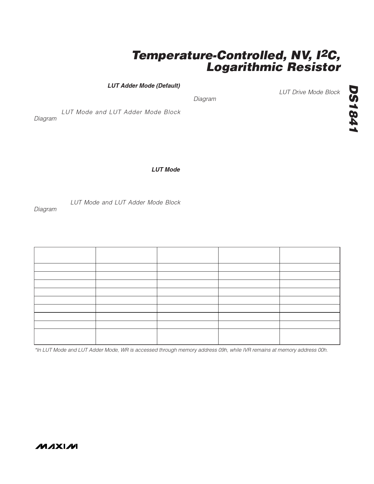
Table 2. LUT Mode and LUT Adder Mode Memory Map
REGISTER
IVR
CR0
CR1
LUTAR
WR
CR2
TEMP
VOLTAGE
LUT
NAME
Initial Value Register
Control Register 0
Control Register 1
LUT Address Register
LUT Value Register
Control Register 2
Temperature Result
Supply Voltage Result
Temperature Lookup
Registers
ADDRESS
(HEX)
00h
02h
03h
08h
09h*
0Ah
0Ch
0Eh
80h–C7h
VOLATILE/NV
NV (Shadowed)
Volatile
NV (Shadowed)
Volatile
Volatile
Volatile
Volatile (Read Only)
Volatile
NV
FACTORY/POWER-UP
DEFAULT
00h
00h
03h
00h
00h
00h
N/A
N/A
00h
*In LUT Mode and LUT Adder Mode, WR is accessed through memory address 09h, while IVR remains at memory address 00h.
_______________________________________________________________________________________ 7
Share Link: 