GS1524A 查看數據表(PDF) - Gennum -> Semtech
零件编号
产品描述 (功能)
生产厂家
GS1524A Datasheet PDF : 16 Pages
| |||
5. Application Information
5.1 PCB Layout
Special attention must be paid to component layout when designing serial digital
interfaces for HDTV. An FR-4 dielectric can be used, however, controlled impedance
transmission lines are required for PCB traces longer than approximately 1cm. Note the
following PCB artwork features used to optimize performance:
• PCB trace width for HD rate signals is closely matched to SMT component width to
minimize reflections due to change in trace impedance.
• The PCB ground plane is removed under the GS1524A input components to
minimize parasitic capacitance.
• The PCB ground plane is removed under the GS1524A output components to
minimize parasitic capacitance.
• High speed traces are curved to minimize impedance changes.
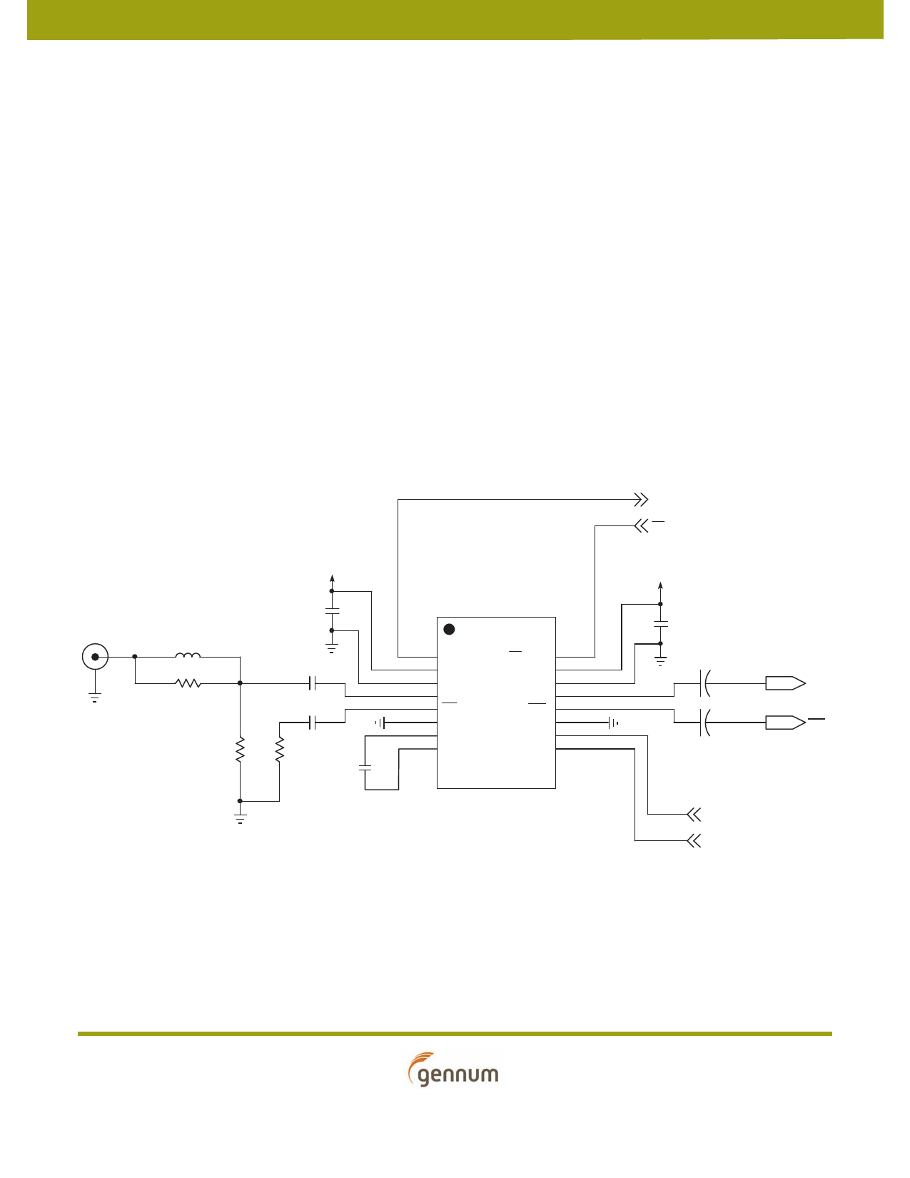
5.2 Typical Application Circuits
CLI
CD/MUTE
VCC
VCC
10n
10n
BNC
6.4n
GS1524A
1 CLI
CD/MUTE 16
1u
2 VCC
VCC 15
3 VEE
VEE 14
+ 4u7
75
4 SDI
SDO 13
1u
5 SDI
SDO 12
+
6 VEE
VEE 11
7 AGC+
MCLADJ 10
75
37.4
8 AGC-
+
BYPASS 9
4u7
1u
SDO
SDO
NOTE: All resistors in Ohms, capacitors in Farads,
and inductors in Henrys, unless otherwise noted.
Figure 5-1: GS1524A Typical Application Circuit
MCLADJ
BYPASS
GS1524A Adaptive Cable Equalizer
Data Sheet
28852 - 5
June 2009
13 of 16
Share Link: 