IL317 查看數據表(PDF) - Integral Corp.
零件编号
产品描述 (功能)
生产厂家
IL317 Datasheet PDF : 2 Pages
| |||
IL317
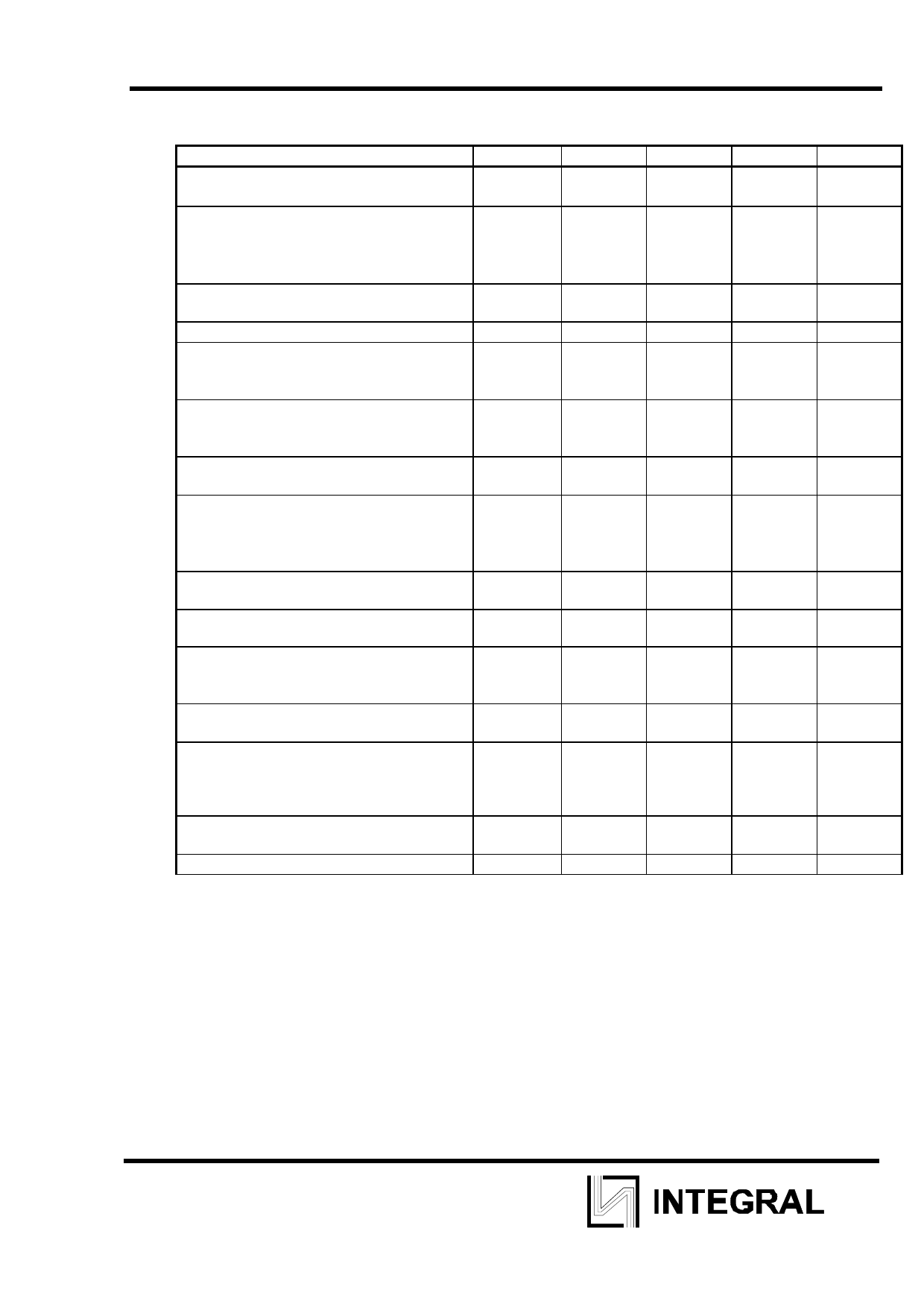
Electrical characteristics
(Vi-Vo= 5.0V, Io = 0.5 A, TJ = Tlow to Thigh (see Note 1); Imax = 1.5 A and Pmax = 20 W unless otherwise
noted)
Characteristic
Symbol
Min
Typ
Max
Unit
Line Regulation (TA=+25°C)
Regline
-
0.01
0.04
%/V
3.0V ≤ Vi - Vo ≤40 V
Load Regulation(TJ=+25°C)
Regload
10mA≤Io≤Imax,
Vin ≤5V
Vin≥5 V
-
5.0
25
mV
-
0.1
0.5
%/Vo
Thermal Regulation (TA=+25°C)
-
-
0.03
0.07
%/W
20 ms Pulse
Adjustment Pin Current
IAdj
-
50
100
µA
Adjustment Pin Current Change
∆IAdj
-
0.2
5.0
µA
2.5 ≤ Vi - Vo ≤ 40 V
10mA ≤IL≤ Imax, PD ≤ Pmax
Reference Voltage (Note 4)
Vref
1.2
1.25
1.3
V
3.0 ≤ Vi - Vo ≤ 40 V
10mA ≤IL≤ Imax, PD ≤ Pmax
Line Regulation (Note 3)
Regline
-
0.02
0.07
%/V
3.0 V ≤ Vi - Vo ≤40 V
Load Regulation (Note 3)
Regload
10mA≤Io≤Imax,
Vin ≤5V
Vin≥5 V
-
20
70
%/V
-
0.3
1.5
%/V
Temperature Stability (Tlow ≤ Tj ≤
Ts
-
0.7
-
Ttigh)
Minimum Load Current to
ILmin
-
3.5
10
mA
Maintain Regulation (Vi - Vo = 40 V)
Maximum Output Current
Imax
A
Vi - Vo≤ 15 V , P ≤ 20 W
Vi - Vo = 40 V, P ≤20W, TA=+25°C
1.5
2.2
-
0.15
0.4
-
RMS Nose , % of Vo
N
-
0.003
-
%/Vo
TA=+25°C, 10 Hz ≤ f ≤ 10 kHz
Ripple Rejection, Vo = 10 V, f = 120 Hz
RR
dB
(Note 5)
Without Cadj
-
65
-
Cadj = 10 µF
66
80
-
Long-Term Stability, Tj = Thigh (Note 6)
S
-
0.3
1.0
%/1.0 k
TA=+25°C for Endpoint Measurements
Hrs.
Thermal Resistance Junction to Case
RθJC
-
5.0
-
°C/W
Notes: (1) Tlow = 0 °C , Thigh = +125 °C
(2) Imax = 0.5 A , Pmax
(3) Load and line regulation are specified at constant junction tempereture. Changes in Vo due to heating
effects must be taken into account separately. Pulse testing with low duty cycle is used.
(4) Selected devices with tightened tolerance reference voltage available.
(5) Cadj , when used, connected between the adjustment pin and ground.
(6) Since Long - Term Stability cannot be measured on each device before shipment, this specification is an
engineering estimate of average stability from lot to lot.
2
Share Link: 