LTC1861L وں¥çœ‹و•¸و“ڑè،¨ï¼ˆPDF) - Linear Technology
零ن»¶ç¼–هڈ·
ن؛§ه“پوڈڈè؟° (هٹں能)
ç”ںن؛§هژ‚ه®¶
LTC1861L Datasheet PDF : 12 Pages
| |||
LTC1860L/LTC1861L
WU
TI I G CHARACTERISTICS The q denotes specifications which apply over the full operating temperature
range, otherwise specifications are TA = 25آ°C. VCC = 2.7V, VREF = 2.5V, fSCK = fSCK(MAX) as defined in Recommended Operating
Conditions, unless otherwise noted.
SYMBOL PARAMETER
tCONV
fSMPL(MAX)
tdDO
Conversion Time (See Figure 1)
Maximum Sampling Frequency
Delay Time, SCK↓ to SDO Data Valid
tdis
Delay Time, CONV↑ to SDO Hi-Z
ten
Delay Time, CONV↓ to SDO Enabled
thDO
Time Output Data Remains
Valid After SCK↓
tr
SDO Rise Time
tf
SDO Fall Time
CONDITIONS
CLOAD = 20pF
CLOAD = 20pF
CLOAD = 20pF
CLOAD = 20pF
CLOAD = 20pF
MIN TYP MAX UNITS
q
3.7
4.66
آµs
q 150
kHz
45
55
ns
q
60
ns
q
55
120
ns
q
35
120
ns
q
5
15
ns
25
ns
12
ns
Note 1: Absolute Maximum Ratings are those values beyond which the life
of a device may be impaired.
Note 2: All voltage values are with respect to GND.
Note 3: Integral nonlinearity is defined as deviation of a code from a
straight line passing through the actual endpoints of the transfer curve.
The deviation is measured from the center of the quantization band.
Note 4: Channel leakage current is measured while the part is in sample
mode.
Note 5: Assumes fSCK = fSCK(MAX). In the case of the LTC1860L SCK does
not have to be clocked during this time if the SDO data word is not
desired. In the case of the LTC1861L a minimum of 2 clocks are required
on the SCK input after CONV falls to configure the MUX during this time.
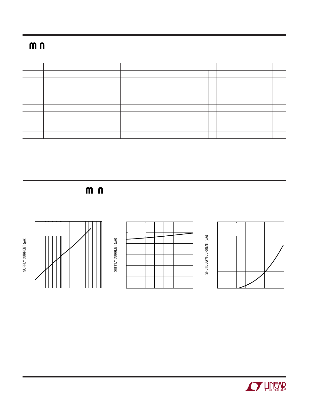
TYPICAL PERFOR A CE CHARACTERISTICS
Supply Current vs Sampling
Frequency
1000
100
CONV LOW = 1.5آµs
TA = 25آ°C
VCC = 2.7V
10
1
0.1
0.01
0.1
1
10 100
SAMPLING FREQUENCY (kHz)
1000
1860L/61L G01
Supply Current vs Temperature
600
fS = 150kHz
VCC = 2.7V
500 VREF = 2.5V
400
300
200
100
0
–50 –25
0 25 50 75
TEMPERATURE (آ°C)
100 125
1860L/61L G02
Sleep Current vs Temperature
20
fS = 150kHz
VCC = 2.7V
VREF = 2.5V
15
10
5
0
–50 –25
0 25 50 75
TEMPERATURE (آ°C)
100 125
1860L/61L G03
18601Lf
4
Share Link: 