MAX4527CSA 查看數據表(PDF) - Maxim Integrated
零件编号
产品描述 (功能)
生产厂家
MAX4527CSA Datasheet PDF : 12 Pages
| |||
Phase-Reversal Analog Switches
__________________Pin Configuration
PIN NAME
FUNCTION
Analog-Switch Input Terminal A.
1
A
Connected to Y when IN is low; con-
nected to X when IN is high.
Analog-Switch Input Terminal B.
2
B
Connected to X when IN is low; con-
nected to Y when IN is high.
Ground. Connect GND to digital
3
GND
ground. (Analog signals have no
ground reference; they are limited to
V+ and V-.)
4
IN
Logic-Level Control Inputs (see Truth
Table).
Negative Analog Supply-Voltage
5
V-
Input. Connect V- to GND for single-
supply operation.
6
Y
Analog-Switch Output Terminal Y.
7
X
Analog-Switch Output Terminal X.
Positive Analog/Digital Supply-Voltage
8
V+
Input. Internally connected to sub-
strate.
Note: A, B, X and Y pins are identical and interchangeable.
Either may be considered as an input or output; signals pass
equally well in either direction. However, AC symmetry is best
when A and B are the input, and X and Y are the output.
Reduce AC balance in critical applications by using A and X or
A and Y as the input, and B and Y or B and X as the output.
_______________Detailed Description
The MAX4526/MAX4527 are phase-reversal analog
switches, consisting of two normally open and two nor-
mally closed CMOS analog switches arranged in a
bridge configuration. Analog signals are put into two
input pins and taken out of two output pins. A logic-
level signal controls whether the input signal is routed
through normally or inverted. A low-resistance DC path
goes from inputs to outputs at all times, yet isolation
between the two signal paths is excellent. Analog sig-
nals range from V- to V+.
These parts are characterized and optimized with ±15V
supplies, and they can operate from a single supply.
The MAX4526 is optimized for high-frequency opera-
tion, and has a higher-speed logic-level translator and
switch driver. The MAX4527 has identical analog switch
characteristics, but has a slower logic-level translator
and switch driver for lower current consumption.
The MAX4526/MAX4527 are designed for DC and low-
frequency-signal phase-reversal applications, such as
chopper amplifiers, modulator/demodulators, and self-
zeroing or self-calibrating circuits. Unlike conventional
CMOS switches externally wired in a bridge configura-
tion, both DC and AC symmetry are optimized with a
small 8-pin configuration that allows simple board lay-
out and isolation of logic signals from analog signals.
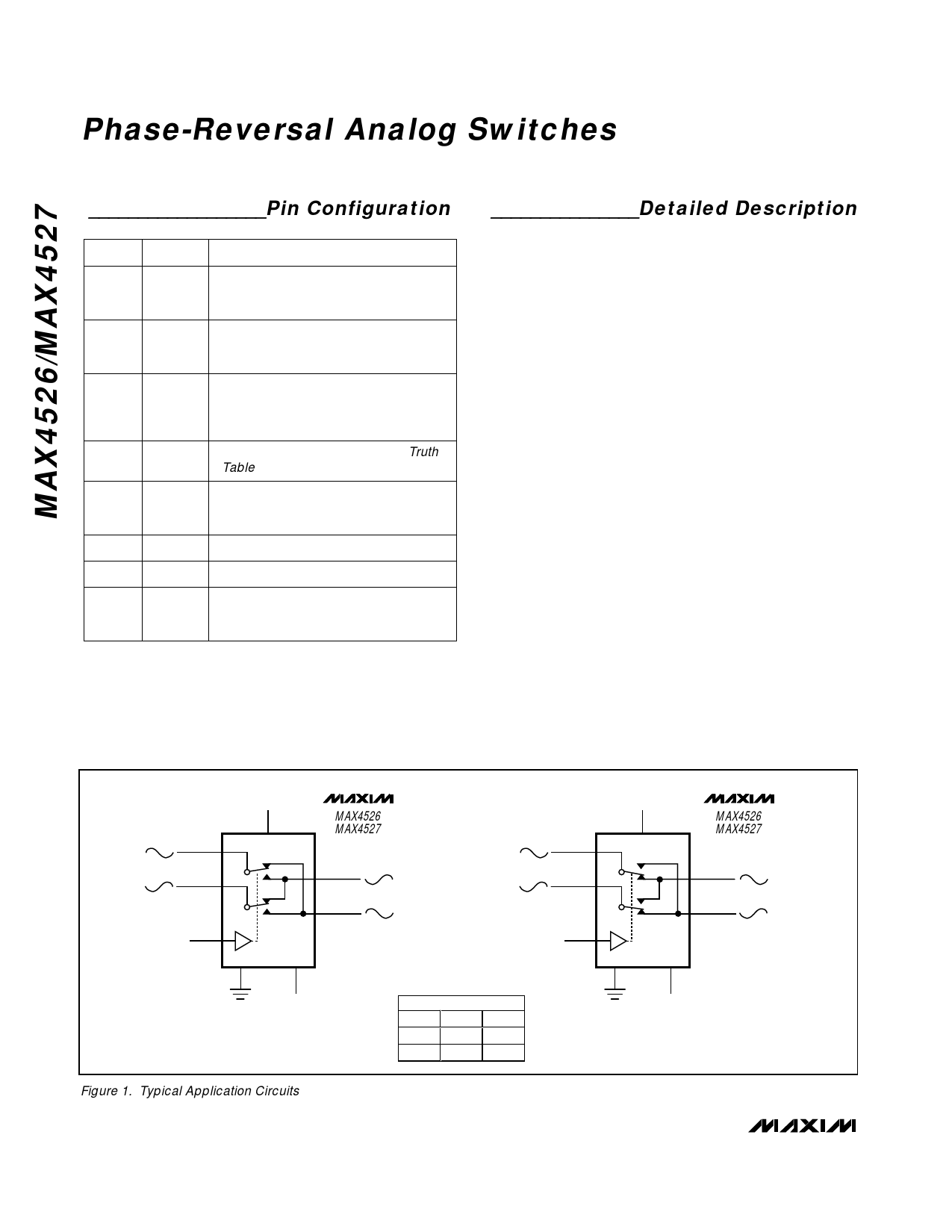
INPUTS
LOGIC LO
V+
A
V+
B
X
Y
IN
GND
V-
MAX4526
MAX4527
OUTPUTS
INPUTS
LOGIC HI
V+
A
V+
B
X
Y
IN
GND
V-
MAX4526
MAX4527
OUTPUTS
V-
TRUTH TABLE
V-
IN
A
B
O
Y
X
1
X
Y
Figure 1. Typical Application Circuits
6 _______________________________________________________________________________________
Share Link: 