MAX8516 查看數據表(PDF) - Maxim Integrated
零件编号
产品描述 (功能)
生产厂家
MAX8516 Datasheet PDF : 10 Pages
| |||
1.425V to 3.6V Input, 1A,
0.2V Dropout LDO Regulators
PIN
MAX8516 MAX8517 MAX8518
1
1
1
2, 3
2, 3
2, 3
4, 5, 10
6
7
8, 9
5, 10
6
7
8, 9
4, 10
6
7
8, 9
—
4
—
—
—
5
—
—
—
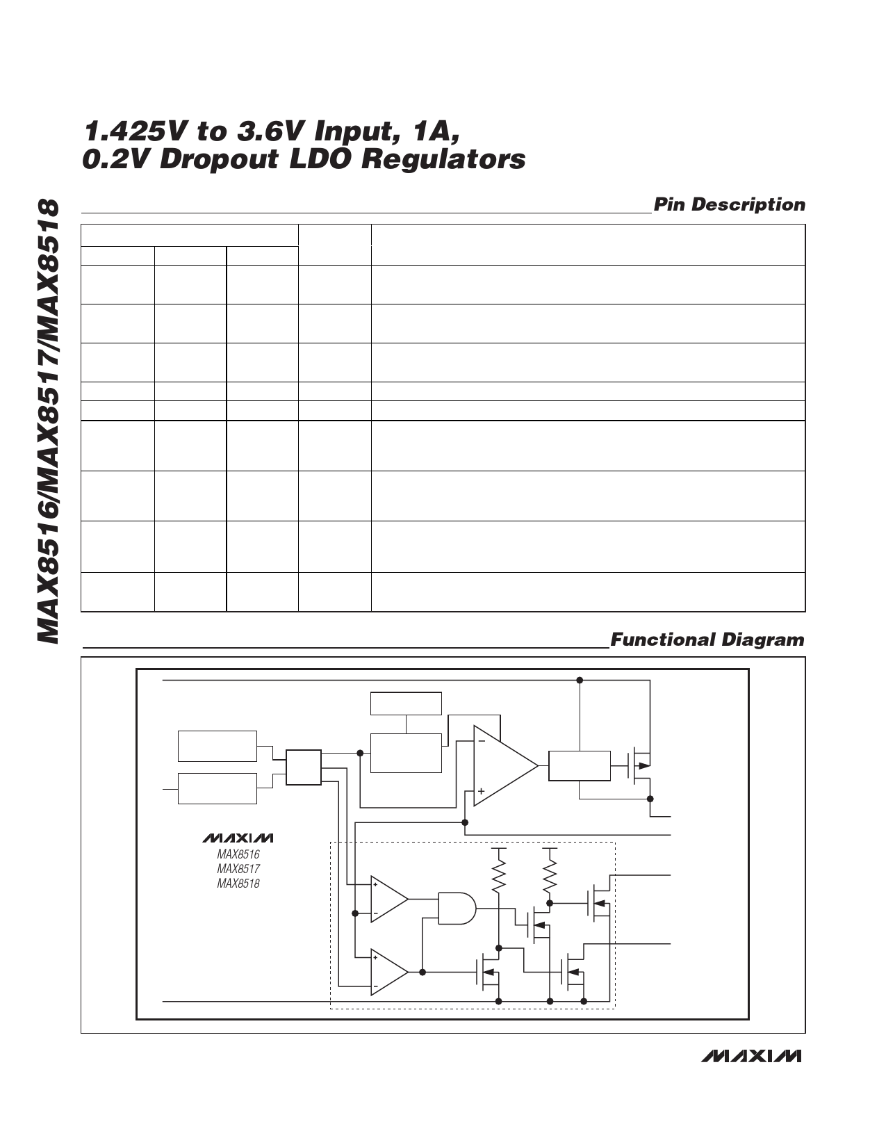
Pin Description
NAME
FUNCTION
EN
IN
N.C.
GND
FB
OUT
POK
POR
EP
Enable Input. Set low to place the device in low-current shutdown mode. Set
high for normal operation.
Regulator Input. VIN can range from +1.425V to +3.6V. Bypass with a 1µF or
higher ceramic capacitor to GND.
No Connection. Pin 10 is internally pulled down to GND with a 10kΩ resistor.
Leave unconnected.
Ground
Feedback Pin. Connect to output through a voltage-divider to set the output.
Regulator Output. Bypass with a 4.7µF ceramic capacitor to GND (a smaller
capacitor can be used if maximum load is less than 1A, i.e., COUT = IOUT
(max) x (1µF/200mA).
Power-OK Output (MAX8517 Only). Open-drain output. Connect to a positive
supply with a pullup resistor. If not used, leave pin unconnected. See the
Detailed Description.
Power-On Reset Output. Open-drain output. Connect to a positive supply with
a pullup resistor. If not used, leave pin unconnected (see the Detailed
Description for more details).
Exposed Pad on the Underside of the Package. Solder to the ground plane for
proper heat dissipation.
Functional Diagram
IN
OVERTHERMAL
PROTECTION
EN
OVERTHERMAL
PROTECTION
THRESHOLD
0.50V
REF 0.55V
0.45V
UNDERVOLTAGE
LOCKOUT
ERROR AMP
WITH
SOFT-START
MOS DRIVER
WITH ILIMIT
MAX8516
MAX8517
MAX8518
OUT
FB
POK
(MAX8517 ONLY)
POR
(MAX8518 ONLY)
GND
6 _______________________________________________________________________________________
Share Link: 