MC74LCX06DR2G(2012) 查看數據表(PDF) - ON Semiconductor
零件编号
产品描述 (功能)
生产厂家
MC74LCX06DR2G Datasheet PDF : 6 Pages
| |||
CAPACITIVE CHARACTERISTICS
Symbol
Parameter
CIN
COUT
CPD
Input Capacitance
Output Capacitance
Power Dissipation Capacitance
MC74LCX06
Condition
VCC = 3.3 V, VI = 0 V or VCC
VCC = 3.3 V, VI = 0 V or VCC
10 MHz, VCC = 3.3 V, VI = 0 V or VCC
Typical
7
8
25
Unit
pF
pF
pF
An
Vmi
tPZL
Vmi
tPLZ
VCC
0V
On
Vmo
VLZ
VOL
PROPAGATION DELAYS
tR = tF = 2.5 ns, 10% to 90%; f = 1 MHz; tW = 500 ns
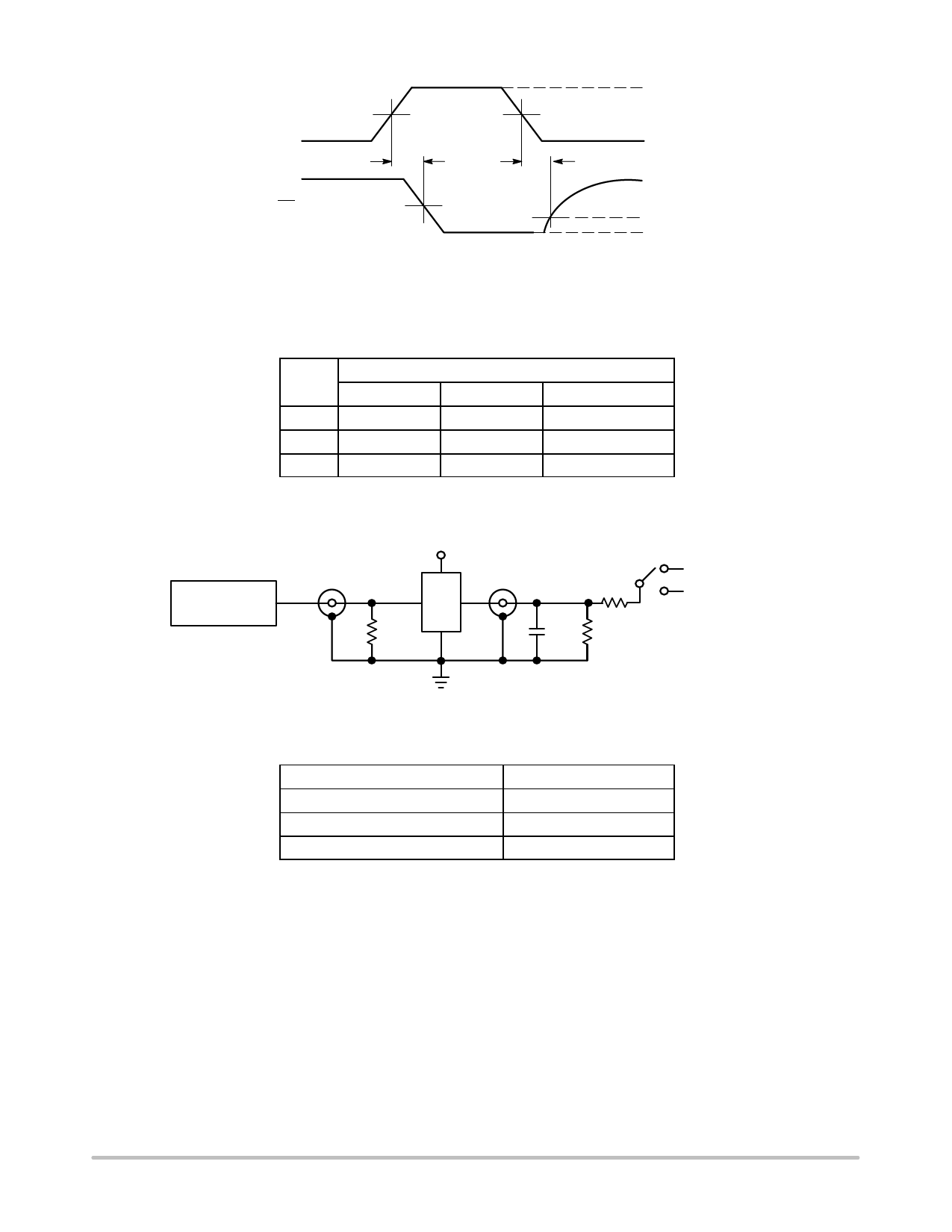
Table 3. AC WAVEFORMS
Symbol 3.3 V $ 0.3 V
VCC
2.7 V
Vmi
1.5 V
1.5 V
Vmo
1.5 V
1.5 V
VLZ
VOL + 0.3 V
VOL + 0.3 V
2.5 V $ 0.2 V
VCC / 2
VCC / 2
VOL + 0.15 V
PULSE
GENERATOR
VCC
DUT
RT
R1
CL
RL
6 V or VCC × 2
GND
Table 4. TEST CIRCUIT
TEST
SWITCH
tPZL, tPLZ
6V
Open Collector/Drain tPLH and tPHL
6V
tPZH, tPHZ
GND
CL = 50 pF at VCC = 3.3 $ 0.3 V or equivalent (includes jig and
probe capacitance)
CL = 30 pF at VCC = 2.5 $ 0.2 V or equivalent (includes jig and
probe capacitance)
RL = R1 = 500 W or equivalent
RT = ZOUT of pulse generator (typically 50 W)
http://onsemi.com
4
Share Link: 