MIC94052(2002) 查看數據表(PDF) - Micrel
零件编号
产品描述 (功能)
生产厂家
MIC94052 Datasheet PDF : 5 Pages
| |||
MIC94052/94053
Absolute Maximum Ratings (Note 1)
Drain-Source Voltage (VDS) .......................................... –6V
Gate-Source Voltage (VGS) ........................................... –6V
Continuous Drain Current (ID) Note 3
TA = 25°C .................................................................. ±2A
TA = 85°C ............................................................... ±1.4A
Pulsed Drain Current (IDP) Note 3 ................................ ±6A
Continous Diode Current (IS) Note 7 ....................... –50mA
Power Dissipation Note 3
SC-70-6 lead (TA = 85°C) ................................... 270mW
Ambient Storage Temperature (TS) ......... –55°C to +150°C
ESD Rating Note 4
Micrel
Operating Ratings (Note 2)
Input Voltage Range ....................................... 1.8V to 5.5V
Junction Temperature Range (TJ) ........... –40°C to +150°C
Package Thermal Impedance Note 3
θJA SC-70-6 lead ............................................... 240°C/W
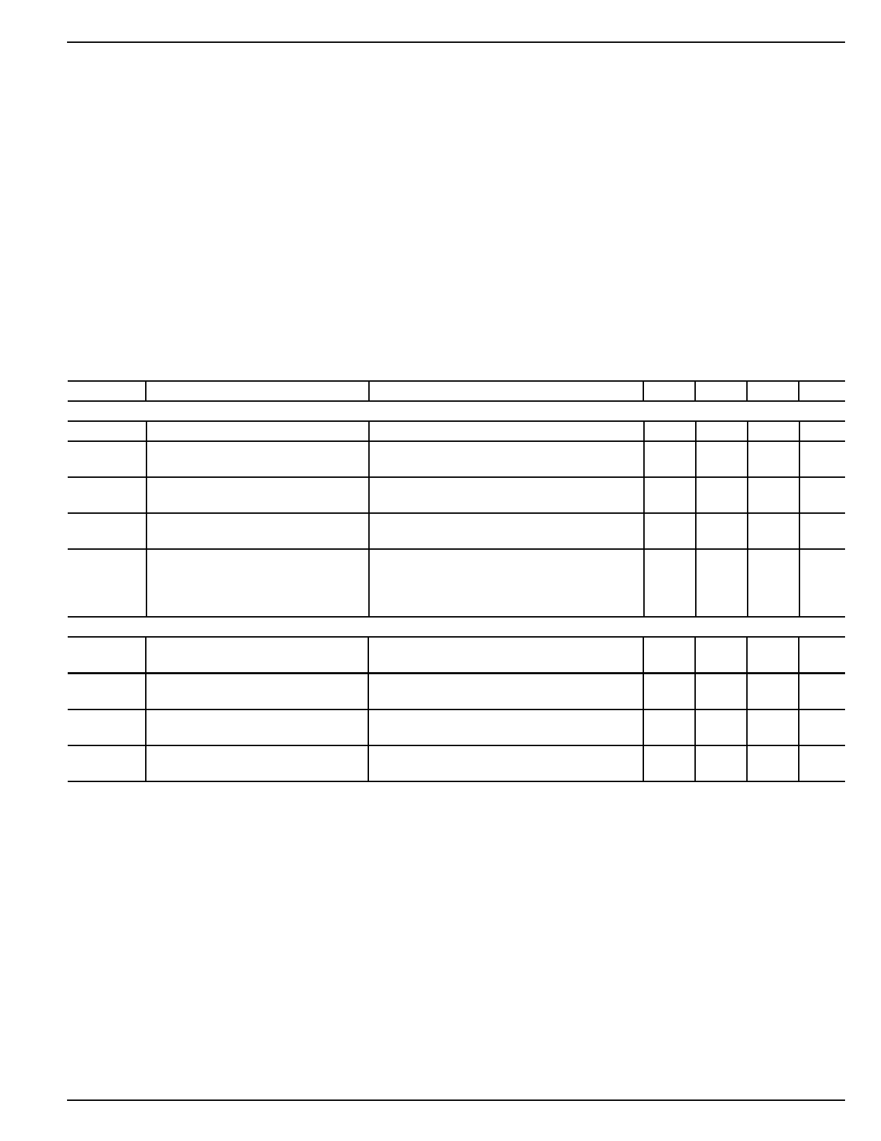
Electrical Characteristics
TA = 25°C, unless otherwise specified. Bold values indicate –40°C ≤ TJ ≤ +150°C.
Symbol
Parameter
Condition
Min Typ Max Units
Static
VGS(th)
IGSS
Gate Threshold Voltage
Gate Body Leakage
(MIC94052 only)
VDS = VGS, ID = –250µA
VDS = 0V, VGS = –5.5V
–0.5
–1.2
V
100 nA
RGS
Gate-Source Resistance
(MIC94053 only)
VDS = 0V, VGS = –5.5V
250 400 550
kΩ
IDSS
RDS(ON)
Zero Gate Voltage Drain
Current
Drain-Source On-Resistance
Note 8
Dynamic, Note 6
VDS = –5.5V, VGS = 0V
TJ = +85°C
VGS = –4.5V, IDS = –100 mA
VGS = –3.6V, IDS = –100 mA
VGS = –2.5V, IDS = –100 mA
VGS = –1.8V, IDS = –100 mA
–1
µA
–5
µA
70
84
mΩ
76
110
mΩ
92
130
mΩ
125 180 mΩ
td(on)
tr
td(off)
tf
Turn-On Delay Time
Turn-On Rise Time
Turn-Off Delay Time
Turn-Off Fall Time
VDD = –5V, ID = –0.5A, VGS = –4.5V,
RGEN = 50Ω
VDD = –5V, ID = –0.5A, VGS = –4.5V,
RGEN = 50Ω
VDD = –5V, ID = –0.5A, VGS = –4.5V,
RGEN = 50Ω
VDD = –5V, ID = –0.5A, VGS = –4.5V,
RGEN = 50Ω
15
ns
15
ns
60
ns
20
ns
Note 1.
Note 2.
Note 3.
Note 4.
Note 5.
Note 6.
Note 7.
Note 8.
TA = 25°C unless otherwise noted. Absolute maximum ratings indicate limits beyond which damage to the component may occur. Electrical
specifications do not apply when operating the device outside of its operating ratings.
This device is not guaranteed to operate beyond its specified operating rating.
Mounted on 1 square-inch pad of 2 oz. copper.
IC devices are inherently ESD sensitive. Handling precautions required.
Pulse test; pulse width = 300µs, duty cycle = 2%.
Guaranteed by design.
Body diode current conduction is not recommended.
Ensure that all drain pins are connected together to optimize RDS(ON) perfomance.
July 2002
3
MIC94052/94053
Share Link: 