NCP4587 查看數據表(PDF) - ON Semiconductor
零件编号
产品描述 (功能)
生产厂家
NCP4587 Datasheet PDF : 19 Pages
| |||
NCP4587
AE
AE
VIN
VOUT
VIN
Vref
Current Limit
CE
CE
GND
Vref
Current Limit
NCP4587Hxxxx
NCP4587Dxxxx
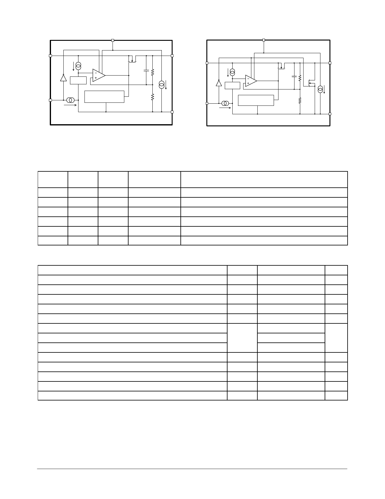
Figure 2. Simplified Schematic Block Diagram
VOUT
GND
PIN FUNCTION DESCRIPTION
Pin No.
XDFN
Pin No.
SC−70
Pin No.
SOT23
4
4
1
2
2
2
3
5
3
6
3
5
1
1
4
5
−
−
Pin Name
VIN
GND
CE
VOUT
AE
NC
Description
Input pin
Ground
Chip enable pin (active “H”)
Output pin
Auto Eco Pin
No connection
ABSOLUTE MAXIMUM RATINGS
Rating
Symbol
Value
Unit
Input Voltage (Note 1)
Output Voltage
VIN
6.0
V
VOUT
−0.3 to VIN + 0.3
V
Chip Enable Input
VCE
−0.3 to 6.0
V
Auto Eco Input
Output Current
Power Dissipation XDFN
Power Dissipation SC−70
VAE
IOUT
PD
−0.3 to 6.0
V
400
mA
400
mW
380
Power Dissipation SOT23
420
Maximum Junction Temperature
TJ(MAX)
150
°C
Storage Temperature
TSTG
−55 to 125
°C
Operation Temperature
TA
−40 to 85
°C
ESD Capability, Human Body Model (Note 2)
ESDHBM
2000
V
ESD Capability, Machine Model (Note 2)
ESDMM
200
V
Stresses exceeding Maximum Ratings may damage the device. Maximum Ratings are stress ratings only. Functional operation above the
Recommended Operating Conditions is not implied. Extended exposure to stresses above the Recommended Operating Conditions may affect
device reliability.
1. Refer to ELECTRICAL CHARACTERISTIS and APPLICATION INFORMATION for Safe Operating Area.
2. This device series incorporates ESD protection and is tested by the following methods:
ESD Human Body Model tested per AEC−Q100−002 (EIA/JESD22−A114)
ESD Machine Model tested per AEC−Q100−003 (EIA/JESD22−A115)
Latchup Current Maximum Rating tested per JEDEC standard: JESD78.
http://onsemi.com
2
Share Link: 