ST3293 查看數據表(PDF) - STMicroelectronics
零件编号
产品描述 (功能)
生产厂家
ST3293 Datasheet PDF : 11 Pages
| |||
ST3293
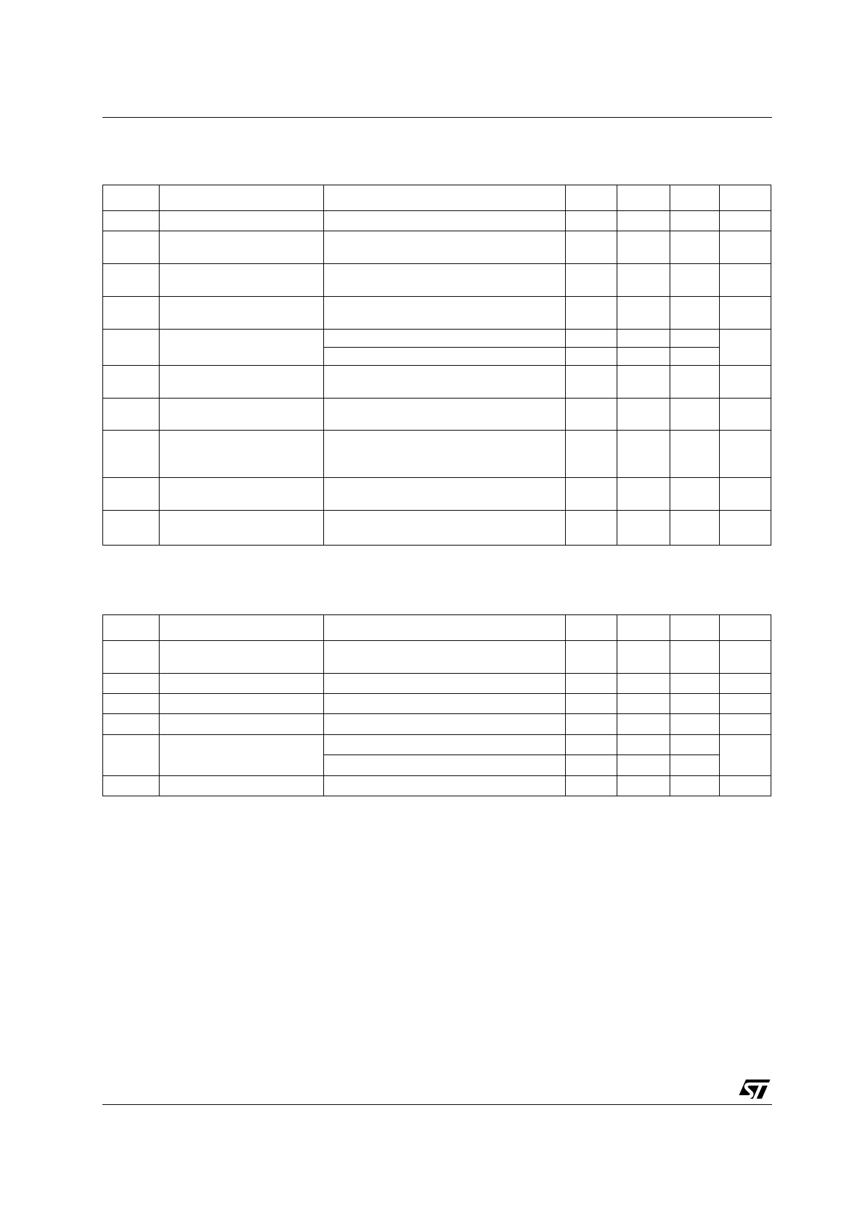
DRIVER ELECTRICAL CHARACTERISTICS
(VCC = 5V ± 5%, -40°C < TA < 85°C, unless otherwise noted. Typical values are referred to Ta = 25°C)
Symbol
Parameter
Test Conditions
Min. Typ. Max. Unit
|VOD|
|VOD1|
DPER
DEF
|VOPD|
Differential Output Voltage
Differential Output Voltage
without Emphasis
Differential Output
Emphasis Step Precision
Differential Output
Emphasis Factor
Differential Driver Output
with Emphasis
∆VOD
VOC
∆VOC
IOFF
IOSD
Change in Magnitude of
Differential Output Voltage
Driver Common-Mode
Output Voltage
Change in Magnitude of
Common Mode Output
Voltage
Output Leakage Current
(Y and Z)
Driver Short Circuit Output
Current
No Load
R = 100 Ω, PE = Low
See Truth Table
See Truth Table
R = 100 Ω, DEF = 1.1
R = 100 Ω, DEF = 1.7
R = 100 Ω, All DEF values
R = 100 Ω, All DEF values
R = 100 Ω
VCC = GND VO = 6V
VO = 0V,
C0 = C1 = C2 = 0
2
VCC
V
2
2.32 2.8
V
0.9
1.1
1
2
2.52
V
3.85
-0.2
0
0.2
V
1
VCC/2 3.5
V
-0.2
0
0.2
V
0.1 ±100 µA
-30
-50 -150 mA
RECEIVER DC ELECTRICAL CHARACTERISTICS
(VCC = 5V ± 5%, -40°C < TA < 85°C, unless otherwise noted. Typical values are referred to Ta = 25°C)
Symbol
Parameter
Test Conditions
Min. Typ. Max. Unit
VTH
VHYST
VOL
VOH
IIN
Receiver Differential
Threshold Voltage
Receiver Input Hysteresis
Low Level Output Voltage
High Level Output Voltage
Input Current
RIN Receiver Input Resistance
-7V ≤ VCM ≤ 7V
VCM = 0V
IOL = 4mA
IOH = -4mA
VIN=10V, Other Input = GND
VIN=10V, Other Input = GND
-7V ≤ VCM ≤ 7V, VCC = 0V
-200
200 mV
50
mV
GND 0.2
0.4
mV
3.7
4.7
VCC
mV
0.32 1.5 mA
-0.5 -2.5
12
24
KΩ
4/11
Share Link: 