SUM110N03-03P 查看數據表(PDF) - Vishay Semiconductors
零件编号
产品描述 (功能)
生产厂家
SUM110N03-03P Datasheet PDF : 3 Pages
| |||
SPICE Device Model SUM110N03-03P
Vishay Siliconix
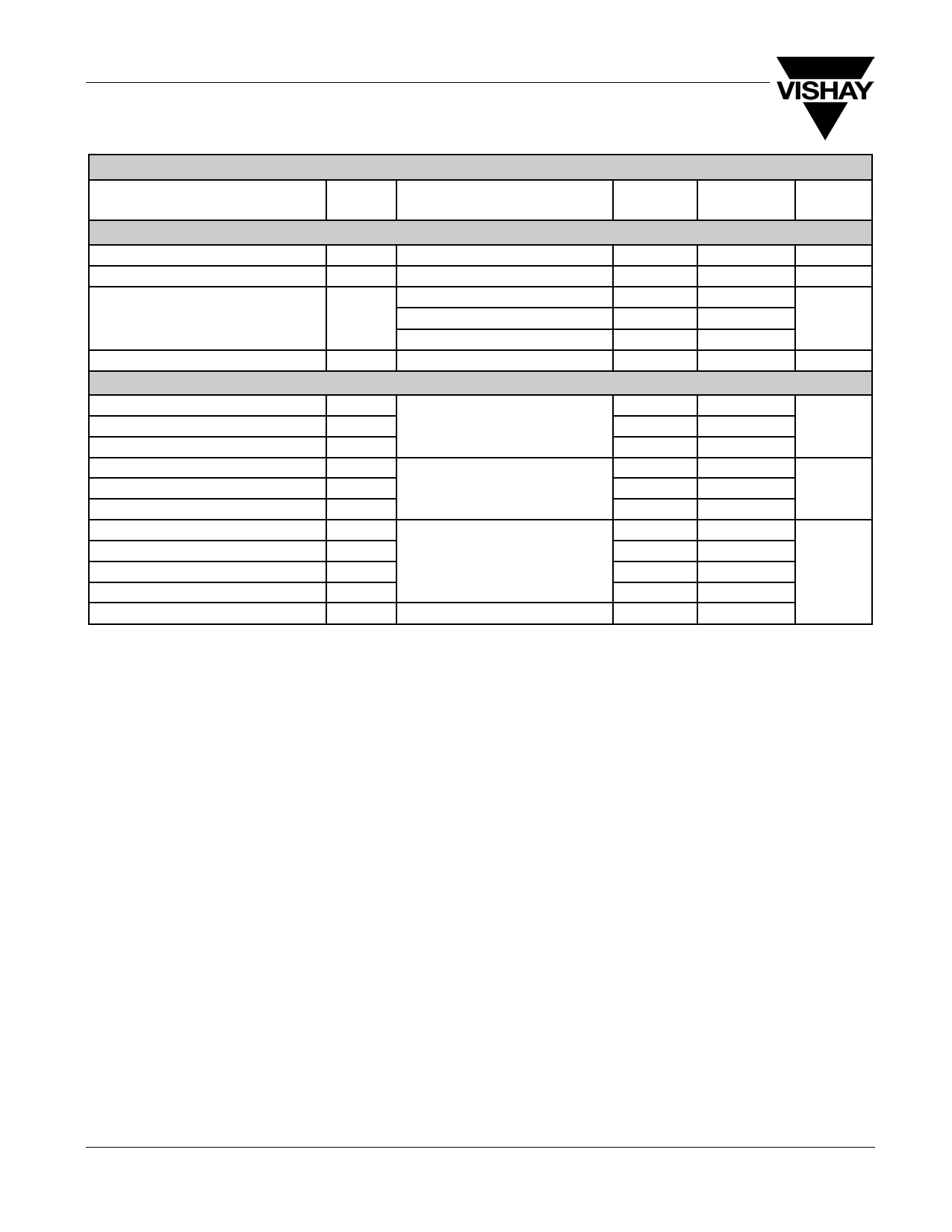
SPECIFICATIONS (TJ = 25°C UNLESS OTHERWISE NOTED)
Parameter
Symbol
Test Conditions
Static
Gate Threshold Voltage
On-State Drain Currenta
VGS(th)
ID(on)
Drain-Source On-State Resistancea
rDS(on)
Forward Voltagea
VSD
Dynamicb
Input Capacitance
Ciss
Output Capacitance
Coss
Reverse Transfer Capacitance
Crss
Total Gate Chargec
Qg
Gate-Source Chargec
Qgs
Gate-Drain Chargec
Qgd
Turn-On Delay Timec
td(on)
Rise Timec
tr
Turn-Off Delay Timec
td(off)
Fall Timec
tf
Source-Drain Reverse Recovery Time
trr
Notes
a. Pulse test; pulse width ≤ 300 µs, duty cycle ≤ 2%.
b. Guaranteed by design, not subject to production testing.
c. Independent of operating temperature.
VDS = VGS, ID = 250 µA
VDS = 5 V, VGS = 10 V
VGS = 10 V, ID = 30 A
VGS = 10 V, ID = 30 A, TJ = 125°C
VGS = 4.5 V, ID = 20 A
IF = 110 A, VGS = 0 V
VGS = 0 V, VDS = 25 V, f = 1 MHz
VDS = 15 V, VGS = 10 V, ID = 110 A
VDD = 15 V, RL = 0.18 Ω
ID ≅ 110 A, VGEN = 10 V, RG = 2.5 Ω
IF = 85 A, di/dt = 100 A/µs
Simulated Measured
Data
Data
1.8
1708
0.0019
0.0026
0.0030
0.93
0.0020
0.0031
1.1
11410
811
498
194
40
40
19
23
50
44
31
12100
1910
1250
172
40
22
20
20
90
25
60
Unit
V
A
Ω
V
pF
nC
ns
www.vishay.com
2
Document Number: 70095
09-Jun-04
Share Link: 